Probably a very silly question but anyway - if the amplifier based on Georgs PCBs is run via XLR, doesn't the buffer buffer only the positive signal?
An externally hosted image should be here but it was not working when we last tested it.
O.K.
that is interesting! I downloaded a Gerber viewer and inverted the bottom side and made a scan of my still unpopulated bottom side pcb and found
yes you are right two longer lines i painted red on the original picture are gone…..
but 🙂 there are instead two small connections in the new layout in the red circles that seem to substitute the long lines….
Please more eyes!
Makes sense Gerd...although i don't like sharp corners in PCB tracks....but maybe that's just aesthetics......
Last edited:
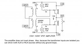
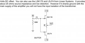
GreatIf I recall, the amplifier's input is simply an isolated transformer primary -
you can connect it any way you like.
😎

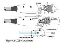
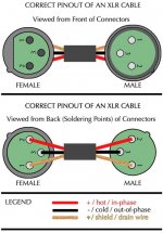
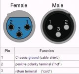
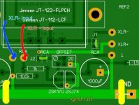
From balanced audio source they are (+) phase (-) phase and shield who go to CSX 1 transformer xlr(+) and xlr(-) input.Probably a very silly question but anyway - if the amplifier based on Georgs PCBs is run via XLR, doesn't the buffer buffer only the positive signal?An externally hosted image should be here but it was not working when we last tested it.
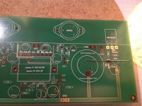
Put jumper on J2 if buffer used.
Ps. Pcb holes for zeners 9,1V 0,5 watt are to small i must redrill them.
With higher diameter can easyer life after next pcb's run 🙂
Greetings
Attachments
-
 29951976-0321-4B3D-9045-F28ED8F0BC49.JPG193.2 KB · Views: 424
 -
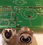 C79D299F-8730-4D5B-BF19-6C706FE7FC73.JPG591 KB · Views: 431
 -
 54608A6C-9FB7-488B-BFB0-C292A6889A83.JPG32.4 KB · Views: 408
 -
 CA414BDF-B95D-4512-9257-8846B5F19F9F.JPG87.1 KB · Views: 213
 -
 9A364F97-9D3A-4B90-990C-B3F23831E8A6.JPG32.3 KB · Views: 192
 -
 34B49A3E-89E1-40B9-8A0C-9DD9816C246B.jpg428.2 KB · Views: 219
Last edited:
Makes sense Gerd...although i don't like sharp corners in PCB tracks....but maybe that's just aesthetics......
THX

@Soundhappy: Yes I have understood what I need to do in order to use the PCB with balanced inputs. My question was - when I look at the PCB the buffer seems to "touch" only the positive signal? What about the negative?
@Soundhappy: Yes I have understood what I need to do in order to use the PCB with balanced inputs. My question was - when I look at the PCB the buffer seems to "touch" only the positive signal? What about the negative?
You are correct that the buffer only 'touches one side of the signal', the buffer itself is single ended. The XLR connections go directly to the xformer and do not pass through the buffer at all.
It is not possible to use the single ended buffer with balanced input as is - in a balanced signal the positive and negative are referenced to each other - not to ground/earth. You cannot connect just the positive because there is nothing then to reference against (and hence no voltage difference to amplify). You cannot connect the negative because there is nowhere to put it - it can never go to ground.
So the options are to not use the buffer and go direct to the xformer, use a balanced buffer on another pcb board if you need a buffer and take the balanced output from that buffer direct to the xformer on Georg's board or use a balanced to single ended transformer at the input of the amp to get a single-ended signal and then feed that into the buffer on the PCB.
If your balanced source has low enough impedance then bypassing the buffer and just going direct to the CSX1 transformer is likely the best option. If not then it may be worth looking for a balanced buffer schematic/kit that you could use.
Ian
Thanks Ian. I'm afraid my preamp has an output impedance of >100 Ohms.
Regards
Sven
Regards
Sven
Last edited:
when you drill through-hole , be sure to solder both sides
Yup thanks ZenMod 🙂
I have today look at on buffer schematic & corespondance with pcb
and for rca input all is connected if jumpers J1 , J2 are close on pcb tracks.
Xlr are not connected at all to the buffer !
J1, J2 is in open pcb tracks position if xlr is used.
I was confused with J2 happily the are smart guys to clarify the things.
Yes it be great option if LSK buffer can be balanced, what modifications ?
Thanks Sven and Ian
Best regards 🙂
Attachments
Last edited:
Ian, I re-read your post and I'm not sure if you are completely right about the balanced signal? In my opinion the positive and negative signals do have a voltage against ground. It would be an option to just use the positive half, however that would of course defeat the purpose of the balanced signal.
Is it possible to add another buffer to the PCB for the "negative" signal? Anybody up for it? 🙂
Regards
Sven
Is it possible to add another buffer to the PCB for the "negative" signal? Anybody up for it? 🙂
Regards
Sven
Ian, I re-read your post and I'm not sure if you are completely right about the balanced signal? In my opinion the positive and negative signals do have a voltage against ground. It would be an option to just use the positive half, however that would of course defeat the purpose of the balanced signal.
Is it possible to add another buffer to the PCB for the "negative" signal? Anybody up for it? 🙂
Regards
Sven
Hi Sven,
After reading some more literature it looks like I was wrong to say that they are only differential to each other.
It is possible to connect the positive to the single ended input.
There is still a question of what to do with the negative - apparently this depends on the output stage of the pre-amp. In many cases this can be tied to ground, but in some cases it cannot and should be left floating.
Ian
Hi Diyers

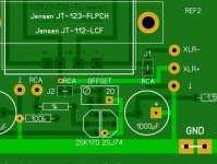
Could with this modifications it work good ?
Jumpers close pcb tracks and gnd is separated from the buffer circuit.
Greetings
Chris
Ian, I re-read your post and I'm not sure if you are completely right about the balanced signal.............?
Regards
Sven
After reading some more literature it looks like I was wrong to say that they are only differential to each other..........?
Ian
Could with this modifications it work good ?
Jumpers close pcb tracks and gnd is separated from the buffer circuit.
Greetings
Chris
Attachments
you can directly feed xformer with balanced signal , in floating mode
if you need buffer prior to xformer - it is SE on the board , so only SE input
for balanced buffered , then you need balanced buffer , which is two SE buffers in fact ....... and you're not having that on board
completely other approach is using stereo F6 in bridged ........ in which case one channel is fed from XLR positive (pin 2) , other from XLR negative (pin 3) , and outputs are taken from channel's hots ........
things are simple ...... when you take them in small steps
Thanks Ian. I'm afraid my preamp has an output impedance of >100 Ohms.
I think you can try up to 600 ohms or so.
😎
For those interested in CSX1 PCBs, we've launched a new GB:
http://www.diyaudio.com/forums/grou...-csx1-sony-vfet-amplifier-30.html#post4121303
http://www.diyaudio.com/forums/grou...-csx1-sony-vfet-amplifier-30.html#post4121303
This is just my point of view...
maybe not possible for jfets input mode.
but just maybe...😀😀😀
maybe not possible for jfets input mode.
An externally hosted image should be here but it was not working when we last tested it.
but just maybe...😀😀😀
Last edited:
To make this board work for either RCA or XLR input, could you use a DPST switch for J1 and J2? I currently use XLR balanced out of my pre-amp, but that could change one day. On my DIY Aleph J I have a switch to ground the pins, but it's not that simple with this board.
Noting ZM's comment about bridged F6s* made me think about bridged Sony VFets so I was looking at the F6 thread again and I noticed that ZM showed a schematic for a F6 using 2sk60 and 2sj18s. Would the 2sk60 and 2sj18 work in CSX1?
My power supplies are up and running although I am using 26-0-26 V transformer I had on hand. Think the heat sink will take the extra heat 😱
Thanks
Bob
* bussforbs Funny 6 is quite the amp IMHO
My power supplies are up and running although I am using 26-0-26 V transformer I had on hand. Think the heat sink will take the extra heat 😱
Thanks
Bob
* bussforbs Funny 6 is quite the amp IMHO
I noticed that ZM showed a schematic for a F6 using 2sk60 and 2sj18s. Would the 2sk60 and 2sj18 work in CSX1?
The Drain resistance seems a little high, but otherwise I think they would
work fine.
😎
- Status
- Not open for further replies.
- Home
- Amplifiers
- Pass Labs
- Article - Sony VFETs part 1