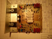
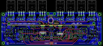
PCB rev 1.2
... I will do as you wish , but right now have no time to do other way.
I will try next week ....🙂 until than are some files attached 😉 and may be somebody will help with another variant .🙄
Alex
... I will do as you wish , but right now have no time to do other way.
I will try next week ....🙂 until than are some files attached 😉 and may be somebody will help with another variant .🙄
Alex
Attachments

Last edited:
... I will do as you wish , but right now have no time to do other way.
I will try next week ....🙂 until than are some files attached 😉 and may be somebody will help with another variant .🙄
Alex
OK Alex thank you, you are very kind, we will see what next week will bring to us.
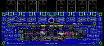
PCB rev 1.3
... I'm back with another layout , I'm convince will have no success , but it's OK for big heatsink in mono block concept .....🙂 I's possible to layout a board with OT in line most common approach , this week or weekend 🙂
Regards Alex
... I'm back with another layout , I'm convince will have no success , but it's OK for big heatsink in mono block concept .....🙂 I's possible to layout a board with OT in line most common approach , this week or weekend 🙂
Regards Alex
Attachments
Last edited:
... I'm back with another layout , I'm convince will have no success , but it's OK for big heatsink in mono block concept .....🙂 I's possible to layout a board with OT in line most common approach , this week or weekend 🙂
Regards Alex
OK Alex, let's wait for that layout.
BR Damir
... I'm back with another layout , I'm convince will have no success
Heat from the power transistors will quickly age capacitors and other components. The up-down temperature changes from the power transistors will shift parameters on other transistors, resistors, diodes, capacitors, etc...
The best circuit stability and reliability requires physically separating the hot high power outputs from almost everything else.
In order to get the best cooling from a physically high heatsink the output transistors can be staggered ---high ___low The pins for the ---high can be at the outer edge of the PCB. The pins for the ___low can be internal on the PCB to where the output mounting screw just clears the PCB edge.
There is a trade off with capacitor heat issues and I don't think it pays to be too conservative about it. The caps need to be close enough to feed the devices and some heat will lower the capacitance ESR. I look at supply caps as consumables that should be replaced every 5 years. I'd rather have an excellent amp during that time than compromised sound for eternity. Keep at it Alex but see if there is a way to make the ground planes wider. I know there are eight devices but trace inductance seems like it might be high (1nH per mm). Does anyone else see it this way?
.... ground traces a bit wider then normal 😀
Cheers ,Alex
Alex you are so fast, you showed different layouts in no time.
If I may suggest some more changes.
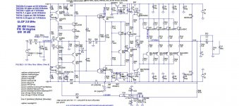
1. When I said distributed elcos are better then the one big I was not clear enough, and my schematic does not show it(attached the corrected one). I think that is better to put one 220uF cap close to each output transistor.
2. Is it possible to have power + - faston connectors on the same side of the board, with double side layout it should be simple, and better if you can have them one above another.
3 Could you move R13 in that way that is connected parallel to the L1 close by with no to much traces between (right side of R13).
4. C18, C19 2.2Uf caps not easy to find in that dimension, I have them with 15 mm space, better to have possibility to use different dimensions.
5. The ground side of the input connector needs one separate ground pin or faston connector to be connected separately to the common star ground outside the PCB.
6. For those who don't wont to use it DC from input to output one input cap can be inserted of 1uF. Could you include that to the layout?
Tank you Alex
Damir
Attachments
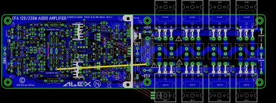
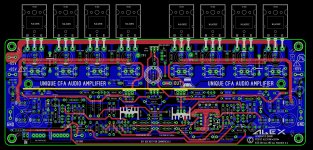
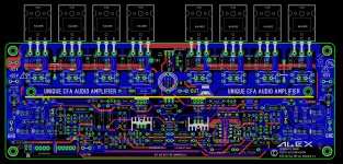
PCB rev 2.2
..... all suggested was done , remains only dimension for 2,2uF capacitors 😉
I'm sorry for this ......
Cheers ,Alex
..... all suggested was done , remains only dimension for 2,2uF capacitors 😉
I'm sorry for this ......
Cheers ,Alex
Attachments
Last edited:
..... all suggested was done , remains only dimension for 2,2uF capacitors 😉
I'm sorry for this ......
Cheers ,Alex
I like it very much. Now is time to check if all is connected as it should be. Maybe some small final adjustment after that.
Best regards
Damir
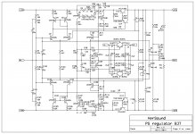
PDF files
I need Q.C. and I think it's easy to check in PDF file , gray color 🙂 (attached)
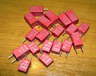
I have some WIMA MKS capacitors small enough at low voltage 63V or 50V 🙂
Regards,Alex
I need Q.C. and I think it's easy to check in PDF file , gray color 🙂 (attached)
I have some WIMA MKS capacitors small enough at low voltage 63V or 50V 🙂
Regards,Alex
Attachments
I need Q.C. and I think it's easy to check in PDF file , gray color 🙂 (attached)
I have some WIMA MKS capacitors small enough at low voltage 63V or 50V 🙂
Regards,Alex
I still need more to check the connections, it is not easy task for my old eyes, but I would like to suggest next:
1. I don't like when high current from the elcos close to the output transistors goes around the input stage and then to the ground. I suggest to widen elcos ground track, remove the -65V connector on the right side and make separate high power ground connector there.
2. R19 should be trimpot of 2kohm for the bias setting. To make more space remove the +-65V connectors between output transistors.
3. I think we don't need those 100uF elcos on the left and right pcb sides now when we have elcos close to the output transistors.
4. Input capacitor C34(C31 on your layout) should be good quality polypropylene type and those came in bigger size than you have on your layout. Could you make a space for bigger one, at least with 15mm connection distance.
5. C18, C19 could be polyester type but still 5mm connection space is to small, add 15mm possibility.
I like added power LED indicators.

cheers Damir
ah yes I forgot, this is 200/400w amp not 120/230W.
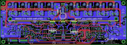
PCB rev 2.3
Thaks you ,voila my last artwork , revised I hope to be OK now ...
Cheers ,Alex
Thaks you ,voila my last artwork , revised
I hope to be OK now ...Cheers ,Alex
Attachments
Last edited:
Thaks you ,voila my last artwork , revised
Cheers ,Alex
I'm sorry for delayed answer, some private business occupies me last few days . Alex you do great layout job, and I think we are very close to the final one.
1. R26 can be of 0.25W type, there not to much dissipation on it. Parallel cap C5 missing serial resistor R99 of 0.22R 0.25W .
2. My bad I did not write on the schematic, C2 can be elcos paralleled with film type(polypropylene) of 100nF. I suggest to live possibility to use pure film type(polypropylene) as it is now on the layout and add possibility to use elcos and parallel small film cap and live to the DIYer to decide what to use.
3. I am repeating my self, C18, C19 (DC servo) with 5mm lead spacing is not easy to find and I suggest to layout for 15 mm lead spacing too.
Still to check all connections is ahead of me.
Cheers, Damir
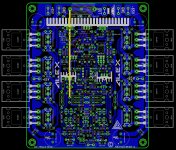
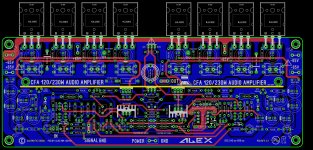
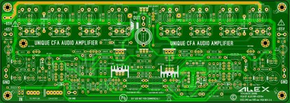
PCB rev2.4
I think it's the final revision of layout , I done everything was necessary /suggested ,even more with personal contribution
Regards,Alex
I think it's the final revision of layout , I done everything was necessary /suggested ,even more with personal contribution
Regards,Alex
Attachments

Last edited:
- Home
- Amplifiers
- Solid State
- Unique CFA 120/230W amp