And this as before but slightly smaller pads...
You GOT IT !!

OS
SlewMonster 5P OPS Final Artwork
OK, to the best of my knowledge we finally have the SlewMonster 5P OPS artwork nailed down. Attached is a zip with the following:
The Sprint layout file
Manufacturing Files - Gerber, Excellon, etc.
DIY Files - PDFs of copper and silk mirrored where appropriate for toner transfer or creating a film
Hope this helps anyone who wants to get into the SlewMonster...
Attachments
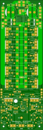
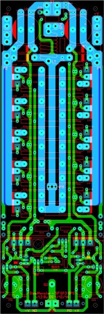
One was just to compare the art I started with and the final version, the other is just the final art. If you don't want the 'dual comparison', just delete that board and save the file.
OK, to the best of my knowledge we finally have the SlewMonster 5P OPS artwork nailed down. Attached is a zip with the following:
The Sprint layout file
Manufacturing Files - Gerber, Excellon, etc.
DIY Files - PDFs of copper and silk mirrored where appropriate for toner transfer or creating a film
Hope this helps anyone who wants to get into the SlewMonster...

Suppose the first singing Spooky...
A little more VAS current ,Pete is this a problem?
A little more VAS current ,Pete is this a problem?
Attachments
Last edited:
Thimios,
A few questions about your build. First off how does it sound?
Is there are reason that you could not put those two devices on the bottom side of the board on top?
Why tin the entire board traces? Wouldn't this make changing a component that much harder to do.
Last question is why didn't you use a connector on both boards rather than only on the IPS section?
Last edited:
Re: SlewMonster 5P OPS Final Artwork
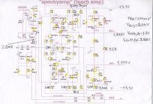
Does this artwork correspond to schematics from post 460 http://www.diyaudio.com/forums/solid-state/248105-slewmaster-cfa-vs-vfa-rumble-10.html#post3829816 ?
Does this artwork correspond to schematics from post 460 http://www.diyaudio.com/forums/solid-state/248105-slewmaster-cfa-vs-vfa-rumble-10.html#post3829816 ?
OK, to the best of my knowledge we finally have the SlewMonster 5P OPS artwork nailed down
Schematic posted in #500 was used, but it is the same at the one in #460. I used what OS posted #1 as the 'reference'.
OK, to the best of my knowledge we finally have the SlewMonster 5P OPS artwork nailed down. Attached is a zip with the following:
Hi Jason,
just a short question: isn't the space you reserved for the fuses a little too "slim", especially with respect to the rather close diodes (D103-D106)?
BR,
Holgi
Hi Jason,
just a short question: isn't the space you reserved for the fuses a little too "slim", especially with respect to the rather close diodes (D103-D106)?
BR,
Holgi
Naf, thimios have even used the "shielded" 10mm fuse holders.
The diodes (reverse prootection/back EMF) are already at potential.
All these "big boy's toys" are well thought out from a perfectionist's
viewpoint. 😀 And they work .. first time (A1 - thimios !! 😎).
OS
Member
Joined 2009
Paid Member
We're safely above 1,000 posts - the race must be half way around the track by now - so who's in the lead at this point, VFA or CFA ? (hint: don't get too serious!)
Suppose the first singing Spooky...
A little more VAS current ,Pete is this a problem?
No problem we can't fix , my friend !!!
(below)
A- I designed 2 resistors into the CCS's Re's. This allows many combinations -
raise the 68R (R10/19) to 82,100,150R ?? .. this will lower CCS current.
Target 8+ total mA for R25/29 (with 3ma through leds) ,
OPS bias should be about midway for optimum bias.
B - brighten up those red leds ... 22-33K should do. This might increase
LED Vf a little , requiring an increase in the value of those resistors in "A"
above. Changing the current of the led's also affects the negative
tempco of the CCS's. The purpose here is to have that tempco offset
the positive one of the LTP's. 🙂
C- You use "evil ceramics" , many a GURU would cringe !! 😀
Use at least 100V multilayer ceramics or preferably silver mica.
This shows the hardiness of the circuit ... it will at least work
with no magic smoke !! 😱
PS - possible "peaking" with standard ceramics at Cdom1/2 ...
OS
Attachments
Last edited:
We're safely above 1,000 posts - the race must be half way around the track by now - so who's in the lead at this point, VFA or CFA ? (hint: don't get too serious!)
I think thimios will find we are "neck to neck".
The design/implementation is as important as the topology.
OS
Hello
Can someone point me where to get KSC/KSA transistors in europe or ebay?
Here in Finland those are impossible to get. I have access to bc and 2n series and I do not want to redraw the ips because of that.
BR,
J
Can someone point me where to get KSC/KSA transistors in europe or ebay?
Here in Finland those are impossible to get. I have access to bc and 2n series and I do not want to redraw the ips because of that.
BR,
J
Hello
Can someone point me where to get KSC/KSA transistors in europe or ebay?
Here in Finland those are impossible to get. I have access to bc and 2n series and I do not want to redraw the ips because of that.
BR,
J
Just look for any with BCE/ECB , post the device # ... and I will
tell you suitability.
Worst case , swap leads of EBC ones with heat shrink tubing
around the base lead.
PS- also Japanese 2sa/sc ECB , as well.
OS
Last edited:
Thanks my friend for this analytic explain.No problem we can't fix , my friend !!!
(below)
A- I designed 2 resistors into the CCS's Re's. This allows many combinations -
raise the 68R (R10/19) to 82,100,150R ?? .. this will lower CCS current.
Target 8+ total mA for R25/29 (with 3ma through leds) ,
OPS bias should be about midway for optimum bias.
B - brighten up those red leds ... 22-33K should do. This might increase
LED Vf a little , requiring an increase in the value of those resistors in "A"
above. Changing the current of the led's also affects the negative
tempco of the CCS's. The purpose here is to have that tempco offset
the positive one of the LTP's. 🙂
C- You use "evil ceramics" , many a GURU would cringe !! 😀
Use at least 100V multilayer ceramics or preferably silver mica.
This shows the hardiness of the circuit ... it will at least work
with no magic smoke !! 😱
PS - possible "peaking" with standard ceramics at Cdom1/2 ...
OS
I will try some modifications tomorrow.
The only reason i has used these cheap ceramics capacitors is that i have only these in my junk box.
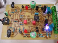
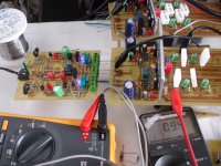
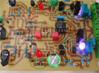
Pete this is a first time work amplifier with these non special parts,thats the important.
Congratulations!

Last edited:
I have put these red capacitors in parallel,one at the top and the other at bottom because i have only 1uf/63V .I haven't any 2u2 non polarized.Thimios,
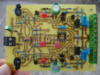
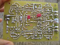
A few questions about your build. First off how does it sound?
Is there are reason that you could not put those two devices on the bottom side of the board on top?
Why tin the entire board traces? Wouldn't this make changing a component that much harder to do.
Last question is why didn't you use a connector on both boards rather than only on the IPS section?
So 1uf//1uf=2uf.
The only reason that i tin boards traces is to protect copper traces from corrosive .My diy pcb haven't solder mask.
Changing a component is easy because parts pins are vertical inserted not twisted.
I have used connector only on the IPS ,it isn't any reason using connectors for both IPS and OUT.It isn't any reason use connectors at all if you don't want changing IPS.
Now i will try answering the difficult question....
How does it sound?
EXCELLENT(My opinion) for this short time listening.
Thimios.
- Home
- Amplifiers
- Solid State
- Slewmaster - CFA vs. VFA "Rumble"