Hi vinodt1347
JP gives some very good hints.
I add mine :
1 - What kind of SPDIF connectors do you use, BNC or RCA type ?
2 - Same question concerning internal wires used for SPDIF connector ?
3 - What is your SPDIF cable lenght & type ?
Regards
Phil
JP gives some very good hints.
I add mine :
1 - What kind of SPDIF connectors do you use, BNC or RCA type ?
2 - Same question concerning internal wires used for SPDIF connector ?
3 - What is your SPDIF cable lenght & type ?
Regards
Phil
I suggest to try a smaller output cap on LT1764 as they dont like too big output caps, something like 100uf.Power supply for the V3 DAC was then switched between the stock LM723 supply or the LT1764. And the results were unchanged from the earlier experiment. Even with the JG filter/buffer, the sound of the LT1764 was fuller and more three dimensional than the stock LM723 supply. The noise of the LT1764 is a bit higher than the LM723, so JP thinks that perhaps I like the sound of noise. But I don't think that's it. There is some dynamic behavior of the LT1764 that is better.
---Gary
A POSCAP 100 µF in parallel to 10 µF X7R is a good combination. At 5V 0 Ohm ESR is OK with LT1764A.
The datasheet doesn't talk much about output capacitance other than to say you need to use at least 10uf. What difference do you see/hear between a big output cap such as I'm using (1000uf) and 100uf?I suggest to try a smaller output cap on LT1764 as they dont like too big output caps, something like 100uf.
Thanks,
---Gary
The datasheet I have goes into output caps in great detail ! I noticed there are a few versions around. Please check.
The device page on Linears' site:
LT1764 - 3A, Fast Transient Response, Low Noise, LDO Regulators - Linear Technology
LT1764 - 3A, Fast Transient Response, Low Noise, LDO Regulators - Linear Technology
Of course, I will!You're welcome.
I hope you will 🙂
Done! Works perfectly! Compared to Benchmark... tried yesterday in the morning, afternoon and end of the day...well...i've got some very weird feeling 😕
There should be a reason of DACs sounding the same. If you don't hear much difference between the stock output of the SB Touch and the Subbu V3 then there is definitely something not going according the plan. Not wanting to be rude but it could also be your hearing. I have a hard time getting used to the need of wearing glasses while my brain thinks I don't need them. Still I have red eyes and a headache everyday 😉
In short, I hear close to zero difference between Subbu and Benchmark, is something wrong?!
Config:
-some usual office Dell %#$@# laptop
-Denon D2000 with pure silver cable and ViaBlue plug
-unmodified Benchmark (not yet 😀)
-1$ usb cable
-just pure Subbu with no preamp/ headphone amp
-Amanero is fed from Subbu PS
I was already tired from switching the cables between those two, but funny thing is that I'm not sure if there is a difference. If there is, it should be negligible small. For instance, I've compared Denons with Sony MDR1 (bloody expensive BT headset) in the morning and it was like day and night, I didn't even try the BT function as it was a complete waste with a cable 😀
Some time later I went to the dacs and was actually surprised with results. Need to say that a month ago or so I compared Benchmark and Subbu on my bookshelf speakers at home (Burmester amp, t+a cd, ASW speakers) and the difference was very obvious and clearly audible. So I though that it's ok for diy project that cost me 10(!) times less than the Bench. Anyway I understand that the Benchmark is not an ultimate dac and my modified t+a cd sounded better in comparison, but still DAC1 is one on the best moderately priced units available now as far as I know and so are the Denons I assume.
So the question is - where the hell is the difference?!😕 Is the Subbu that good pared with Amanero or perhaps headphones does not require that detailed and hi-endish sound as stereo configs?!
I'll make some more tests in a different manner, perhaps I should try some long term comparisons like listening for several days to one dac and switch then to another.
tested with metal music.
Attachments
Last edited:
Hi dtses
Thank you for your feedback 🙂
I'm interrested in your Amanero's fed from Subbu/JP PSU.
I'm using this config with an Isolator but hadn't modded Amanero's PSU.
Great and nice job !
Regards
Phil
Thank you for your feedback 🙂
I'm interrested in your Amanero's fed from Subbu/JP PSU.
I'm using this config with an Isolator but hadn't modded Amanero's PSU.
Great and nice job !
Regards
Phil
The first problem I can see is the I2S being transferred through the ribbon cable and the return (GND) connection. It is far from optimal and could cause far from optimal signal integrity, especially with the clock. The GND connection should be as close to where the signals join the board as physically possible. Each line would be better transferred as a twisted pair with the GND (return) joining at the closest point. If this is not possible, then the clock as the most critical signal should be in the next wire to the GND ; and that GND connected as near to the clock entry point as possible.
This article from Henry Ott is a light hearted look at the problem (the first two points apply here), it does refer to EMC, but you must remember that EMC and signal integrity are two sides of the same coin (signal integrity problems are EMC issues between a PCBs own signals and return path).
The 10 Best Ways to Maximize Emission from Your Product
Some more relevant articles on clocks, jitter and return paths…
Staying Well Grounded
http://home.educities.edu.tw/oldfriend/article/SI/Crosstalk_Induced_Jitter.pdf
http://www.ti.com/lit/an/slyt179/slyt179.pdf
Marce
Thank you for your usefull informations as usual
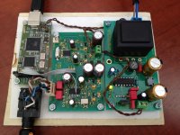
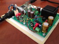
As you can see, Subbu DAC V3 isn't an I2S but a SPDIF only version.
BTW there are no GND return path from I2S lines on this PCB.
For me, the closest Digital GND is Pin14, near clock. (maybe I'm wrong)
Maybe you can point us a better location ?
Many thanks for your articles, takes some times... 🙂
Regards
Phil
Thank you for your usefull informations as usual
As you can see, Subbu DAC V3 isn't an I2S but a SPDIF only version.
BTW there are no GND return path from I2S lines on this PCB.
For me, the closest Digital GND is Pin14, near clock. (maybe I'm wrong)
Maybe you can point us a better location ?
Many thanks for your articles, takes some times... 🙂
Regards
Phil
Last edited:
C21 looks closest, interestingly the beta layout shown on the first page of this thread had connectors X3-X5 next to the resistors, which would have been perfect as they look like these sort of sockets:
1055688-1 Product Details - TE
so would have been perfect for utilising I2S.
The other option is to drill a little hole for the wire through the board, clean some resist from the GND plane and solder the lead to that.
Ribbon cables such as those that we use to use in their thousands years ago are the worse cables for EMC when used with digital, hence their appearance only in cut price products these days.
Sorry I haven't answered your email yet, I've had a horrible last couple of weeks, and its only going to get worse as I am on site at a customers premises from this weekend for a few weeks (sunny Harrow, so 9 hours comuting each week as well as a full weeks work!)
. . . interestingly the beta layout shown on the first page of this thread had connectors X3-X5 next to the resistors, which would have been perfect as they look like these sort of sockets:
1055688-1 Product Details - TE
so would have been perfect for utilising I2S.
Actually the board is set up to use u.fl connectors such as this http://www.hirose.co.jp/cataloge_hp/e32119372.pdf
---Gary
Pedant😀
There were RF connectors now there are not.......Also footprint has one to many pads for U.fl connectors since we are being picky today🙂
There were RF connectors now there are not.......Also footprint has one to many pads for U.fl connectors since we are being picky today🙂
Marc,
You do like to argue, don't you 😉.
As one who built one of the V3 beta boards and who has a copy of the recommended parts list for that board, I feel fairly confident in my comments.
Just curious - have you built one of these yet? I saw some board designs you were spinning up. Would be curious to see how those compare to Subbu/JP's version, which can be taken to a pretty high level.
---Gary
I am not arguing, I looked at the footprint, it has four pins so I just commented on a four pin RF connector, the ones you referenced are actually a 3 pin footprint that is all.
I design boards with a variety of RF connectors regularly, more so than most as I spend my days doing PCB designs.
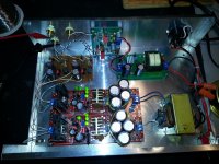
The board design I am doing will have the same parts exactly as JP/Subbu's schematic, unless either design was flawed (mine or the original), which neither are then there will be no difference in the output. The only thing I decided to give myself a challenge was to limit the rear of the board to just the GND/0V/Return, this I have achieved apart from the -15V of the JG Buffer, all I have to do is change my SMD caps to 0805s and move the circuit blocks out to create room for the PTH components.
The layouts I am doing are mainly for fun for my own enjoyment, but all version will be available to who ever wants them, or not as the case may be, I am having fun, and the community can benefit from that, which is what all this DIY is about. The final version will be home makeable, ie largish vias GND only to the bottom layer.
And look on the bright side, you get my expertise with all aspects of PCB design, assembly and fabrication for nothing, good value; 🙂
I design boards with a variety of RF connectors regularly, more so than most as I spend my days doing PCB designs.
The board design I am doing will have the same parts exactly as JP/Subbu's schematic, unless either design was flawed (mine or the original), which neither are then there will be no difference in the output. The only thing I decided to give myself a challenge was to limit the rear of the board to just the GND/0V/Return, this I have achieved apart from the -15V of the JG Buffer, all I have to do is change my SMD caps to 0805s and move the circuit blocks out to create room for the PTH components.
The layouts I am doing are mainly for fun for my own enjoyment, but all version will be available to who ever wants them, or not as the case may be, I am having fun, and the community can benefit from that, which is what all this DIY is about. The final version will be home makeable, ie largish vias GND only to the bottom layer.
And look on the bright side, you get my expertise with all aspects of PCB design, assembly and fabrication for nothing, good value; 🙂
LOL
Sorry, neither am I.
I want to finally build a few of theses to go with the squeezeboxes we have, the initial version I want to play with would be all SMD as shown earlier, with a USB connector for +5Vs (D-+ not connected) from a USB charger of some sort. It gives an initial easy build, easy powered cheap board to practice on, and get a reasonable sound. The other version is the full blown customisable one, with PSU, JG Buffer and probably some a basic +-15V regulators, the basic layout was uploaded earlier, again I want single sided signals, GND plane bottom layer (some strategic cuts to minimise the digital sides effect on the analogue output, but allowing a low impedance connection for any HF mush to return from any filters). It will also be designed to have the PSU section removable for any who want to use an alternative power supply.
🙂
The layouts I am doing are mainly for fun for my own enjoyment, but all version will be available to who ever wants them, or not as the case may be, I am having fun, and the community can benefit from that, which is what all this DIY is about.
It would be nice if you asked us first if we like our design being available in a copied/improved/changed version (better or not, is not relevant here). When you asked for it I sent the schematics to you as you wanted to do your own PCB design which is fine. You never stated the PCBs or the design would be available to others.
Last edited:
- Home
- Vendor's Bazaar
- Modifying the Subbu V3 DAC