. Then again, the result can be deduced from the PSRR plot. If you apply a 6 kHz, 1 V sine wave to the VEE supply, you should get 1 mV on the amp output (60 dB PSRR). If you want to predict the effects of a triangle wave, look up the Fourier series, figure out the harmonics, and do the math.
~Tom
It's my understanding you must subtract the closed loop gain from the PSRR curve to obtion the magnitude of reduction seen at the output. So in typical applications it will be much less than 60dB you quote.
The conservative practice should be to estimate PS ripple using the CMRR curve instead of PSRR curves for balanced PS's on LM3886 eg worst case. So a single supply does have some advantages there.
Last edited:
Sorry, just frustrated, nobody seems to be able to prove that PSU design influences sound, just many claims that is does.
Certainly that's an incorrect statement based on my own experience. I've seen people describe the effect of improving power supplies on their amp. My description of the sound from improving the power supply on my chipamp turns out largely to tally with theirs. So its not merely a claim, rather a description of the contents of our perception. Sure there are some people who just claim 'it sounds better' but they don't represent all folks who tinker with supplies on chipamps.
I believe all these claims, where is the data to back it up? Tomchr tweaked his design and got measurable improvement.
I started my own thread, like here the discussion goes to PSRR and many even claimed that the PSU doesn't effect sound.
It would be great to see if PSU design affects Distortion, Bandwidth, Frequency Response, Gain, etc..
I started my own thread, like here the discussion goes to PSRR and many even claimed that the PSU doesn't effect sound.
It would be great to see if PSU design affects Distortion, Bandwidth, Frequency Response, Gain, etc..
Last edited:
The DS shows the PSRR only for open-loop operation. It would be instructive to see what happens when the loop's closed. When I tried simming the LM3886 schematic for PSRR in LTspice (closed loop) I couldn't reach the theoretically predicted performance at the lowest frequencies.
<edit> when I wrote 'a wideband noise' I wasn't sufficiently clear. I didn't mean to say that the supply ripple was the same as wideband noise. It isn't - for a single sinewave output its discrete harmonics. It approaches noise-like characteristics for music though.
one could build a linear regulator and see if they hear a difference, heck you could run it off a single supply just the +Vcc rail too , so you get tons of clean PSRR power. ala http://www.akitika.com/measurements.html
example of a regulated power supply for stereo LM3386 http://www.updatemydynaco.com/documents/AssemblyManualPowerSupplyReplacementRev2p06.pdf
Last edited:
Yes I went over to single supplies for my amps over a year ago, haven't looked back. Building capacitor arrays now - would be twice the work-up if I needed two capacitor arrays for every amp! I have seen that Akitika amp before and it looks like the designer really thought about the supply issues, a very reasonable price too for a kit.
It's my understanding you must subtract the closed loop gain from the PSRR curve to obtion the magnitude of reduction seen at the output.
I see where you're coming from. Assuming the PSRR is the result of the loop gain reducing the supply disturbance, you would need to take the loop gain reduction of a circuit with higher closed loop gain into account when figuring the PSRR of the complete amp. However, if you're building an amp with a gain of 20 V/V (26 dB), you'll get the PSRR published in the data sheet as it's measured at 20 V/V. I'm 99.999 % sure of this.
Note that the PSRR spec in the table is measured using the DC circuit. I.e. it's the PSRR at 0 Hz...
I believe all these claims, where is the data to back it up?
+1
When you modify a circuit, it is very easy to hear a difference between before and after. In many cases, that's the result of expectancy bias. Your ears also took a break between "before" and "after". Then you add the built-in vagueness of "audio speak". How many veils have been lifted? How sonically transparent were these veils exactly? Some people will describe a sound as harsh (negative quality) whereas others describe the same sound as precise (positive quality).
It gets worse when multiple people are involved as they tend to affect each other. This has been demonstrated countless times by psychologists. Unless you conduct a double or triple blind test on a large subject pool, I would argue that it is very, very hard to get good data in a listening test.
Also, don't forget that people have different preferences for sound quality. I'm right now listening to my Damn Good 300B Amp. Four 300B tube channels in a vertical bi-amp configuration. To my ears it sounds heavenly. The THD at 1 kHz, 1 W is 0.3 % rising to 3 % at 10 W.
At least if you measure a change in an amplifier parameter after a circuit change, you can determine causation. You can also determine if your circuit change had an effect on the parameter you're measuring. I prefer to correlate the change in a measured parameter to a change in perceived sound quality rather than the other way around.
It would be great to see if PSU design affects Distortion, Bandwidth, Frequency Response, Gain, etc..
From my experience designing op-amps: The gain-bandwidth product and, hence, frequency response, gain is a relatively weak function of the supply voltage. By far the biggest contributor is process variation followed by temperature. Supply voltage is pretty far down the list. This holds until you lower the supply to the point where the amp browns out.
I think it would be interesting to look at the output spectrum with supply wiggle applied.
I'll get the data for you. Stay tuned. Just don't expect it to happen overnight... 🙂
~Tom
Last edited:
To Tomchr,
what does make a good Chip-amp?
I am starting to see these Chip-amps as a feedback loop with a network of current supplies. The actual op-amp only impacts through its differential inputs and protection circuits.
what does make a good Chip-amp?
I am starting to see these Chip-amps as a feedback loop with a network of current supplies. The actual op-amp only impacts through its differential inputs and protection circuits.
This thread is very informative and interesting.
Thank you so much Tomchr, For the time you have put into this!!! 🙂
Quite some time ago I had asked "What is ones favorite or the best type of configuration (schematic) to use with the LM3886" and I never got a solid answer only to be asked the same question back at me "What is yours?" and I simply replied " I don't have one, I just want one that works!!".
What was confusing to me was, How many people have used the same basic schematic and some have gotten great results and many others have complained about the results they have gotten.
I knew there had to be more to this than just the components being used as some had went and spent the big bucks on premium parts and still got bad or mediocre results, as it is not much different than your basic opamp design!!!
Then there is the threads about change this and change that and again some results were marginal.
I just wanted to build one and have it work the way it is supposed to work without having to spend $20 on a set of boards that I can make myself for less than a $1 or two.
So therefore I have yet to wire one up.
Or even make a board because there are so many differing opinions about how it sounds with different board layouts from different sources!!
This thread certainly explains a lot of the why's and how to go about a good layout that works.
I now see the Light!!!! 😉
Thank you for your work as the info in this thread gives me the info and confidence I needed to start a massive chipamp project of my own that has been in the planning stages for nearly 10 years!!
And make it sound Good!!! 😉
Cheers!!!
jer 🙂
If you outline your understanding of the science behind why the performance should be better with the input ground (black wire) connected to the star ground by the other passives rather than the star by the supply caps, I'll be happy to move it and retake the measurements.
The point between supply decoupling capacitors (even local ones) carries rectified current from the class-AB output stage. Star ground point must not be placed here...
I think the most important thing is to have one star ground reference for the circuit. If your main supply caps are right on top of the LM3886, the ground star can be between them. But if the caps are off some place (as they tend to be due to their size), you're better off creating a local ground star at the LM3886 local decoupling and running a wire from there to the center between the caps. My measurements show that quite clearly (look a few pages back).
~Tom
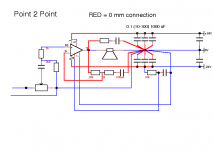
Hi Tom, I checked my construction notes and this is what I did.
Main star is a bolt in the middle of the PS board with various returns bolted together.
Zero volts from xformer first lug on star point on PS
Speaker returns next lug on star point on PS
Decoupling caps and mute cap grnd next lug on star point on PS
zobel cap returns next lug on start point on PS
Pin7, Neg Feedback Cap, input gnd and input ground ref resistor (all connected on pin 7) last lug on star point on PS
You said that the zobel cap return made the biggest difference (I think). When I did my p2p I thought long and hard about it (based on the datasheet) and that was what I came up with. I figured that input, Neg Feedback and the zero volts reference of the chip were probably best all locally tied on pin7 and that the others (due potentially high currents) should go direct to the star point on the PS PCB. I'm now wondering about the zobel cap...
I'm going to need to make a decent balanced to unbalanced converter before I can do good distortion measurements as my focusrite 2i2 has poor performance when the balanced output is feeding an unbalanced load. But I am interested to try and get some measurements to see how the thing behaves at higher frequencies.
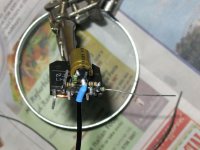
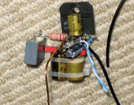
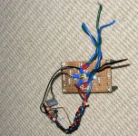
Couple of pics attached showing where things were with relation to the chip 🙂
edit: looking back at your post, I think what I did was basically closest to your IN+FB long ground. The main difference is my main star point is in the middle of my PS board, You said that you should not do this! It wouldn't be very hard for me to make a second star point and bolt all of those coming from the chip there, and then run a separate lead to the PS star point..... added pic of ps board as well...
Tony.
Attachments
Last edited:
If you outline your understanding of the science behind why the performance should be better with the input ground (black wire) connected to the star ground by the other passives rather than the star by the supply caps, I'll be happy to move it and retake the measurements............... and, preferably, outline the reason for your suggested changes. Referring to some arbitrary "best practices" doesn't carry much weight, honestly.
To me, the circuits are functionally identical. Neither circuit shows issues with stability or ground loops. If you know of any scientific explanation of why changing the grounding will improve the HF THD, I'm all ears. Right now what I'm hearing is "this doesn't follow "best practices" (whatever that might be)" without any explanation of how you would prefer the layout to be and why your "best practices" will improve the performance of the circuit.
I'm all about discussing the circuit and the layout. But please back you claims up with a logical explanation based in science so we can keep the debate scientific ...........
...............The results were rather dramatic.
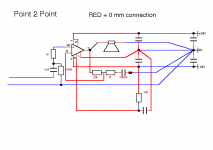
Conclusion: Layout matters greatly - also in P2P wiring (we knew that). I achieved the best performance with the IN and feedback (FB) grounds combined and returned together to the star ground. Separate IN and FB ground returns were slightly worse. Star grounding, actually, a little bit worse that the other two. NO ground return should return separately to the center point between the supply caps. Run only one wire from the ground star to this point.
Moving the Zobel network to sit directly from the IC pin to the ground star made by far the biggest improvement, closely followed by moving the IN ground to the ground star as well. That was the reason for the poor performance I was getting. My bad... The schematic for the UNOPTIMIZED P2P tested yesterday (the gray trace in the attached graph) can be found in Post #14. The Zobel network was connected across the speaker terminals (don't do that!!).
I will take the lessons learned from this and apply them to my PCB design..........
You rejected my input.I think the most important thing is to have one star ground reference for the circuit. If your main supply caps are right on top of the LM3886, the ground star can be between them. But if the caps are off some place (as they tend to be due to their size), you're better off creating a local ground star at the LM3886 local decoupling and running a wire from there to the center between the caps. My measurements show that quite clearly (look a few pages back)............
Why, because you needed the scientific explanation behind any suggestion.
Yet you now accept that layout does have a profound influence on performance.
Low Loop Area is crucial to ALL circuits
How more simple does the science need to be?
Last edited:
Hi wintermute,
I think this is close to what you made. Some interesting choices.
I think this is close to what you made. Some interesting choices.
Attachments
Last edited:
HiI see where you're coming from. Assuming the PSRR is the result of the loop gain reducing the supply disturbance, you would need to take the loop gain reduction of a circuit with higher closed loop gain into account when figuring the PSRR of the complete amp. However, if you're building an amp with a gain of 20 V/V (26 dB), you'll get the PSRR published in the data sheet as it's measured at 20 V/V. I'm 99.999 % sure of this.
Note that the PSRR spec in the table is measured using the DC circuit. I.e. it's the PSRR at 0 Hz...
<snip>
From my experience designing op-amps:
<snip>
~Tom
according to the TI data sheet the definitions of CMRR and PSRR refer to the input NOT the output. It just doesn't make sense for an op-amp to define the PSRR at the output at a set gain. why? it's not user friendly, is that normal practice in your experience designing op-amps? how does the user predict the PSSR results at any CL gain greater than 10V/V?
Common-Mode Rejection: The ratio of the input common-mode voltage range to the peak-to-peak change in input offset voltage over this range.
Power Supply Rejection: The ratio of the change in input offset voltage to the change in power supply voltages producing it.
the DC test circuit #1
as I see it , the null circuit increases open loop gain and the CL gain is 500V/V. also seems the DC null circuit keeps the output from referencing ground at 0V?
maybe you can explain the open and closed loop gains and how that is used produce meaningful data at 20V/V , I can't see it. Is there a #2 DC test circuit?
Last edited:
This thread is very informative and interesting.
Thank you so much Tomchr, For the time you have put into this!!! 🙂
Thank you for the recognition.
Quite some time ago I had asked "What is ones favorite or the best type of configuration (schematic) to use with the LM3886"
Sorry to be a bit on the blunt side here, but as you can figure from the past seven pages of this thread, you're not really asking the right question, hence, aren't get a very satisfactory answer. Classic communication issue... 🙂 All the measurements I've posted have used the same circuit schematic (except the change from inverting to non-inverting for that comparison). The layout makes the difference - and the difference is rather stark.
A better question would probably be, "which schematic should I use and how should I build the layout?". But that opens up a can of worms... There are many opinions on what a "good layout" means and few have the data to back it up.
Then there is the threads about change this and change that and again some results were marginal.
I share your frustration. Many of those threads go: "I've built the LM3886 following this schematic, it sucks. How can I make it not suck?" That's typically followed up by one of these standard responses,
- OMG!!! You've forgot the NOT OPTIONAL stability components (the extra Rf2, Cf, and Cc in the AC Test Circuit in the data sheet). IT'LL BLOW UP IN YOUR FACE!!
- You probably have a fake LM3886. You should buy from a TI/National distributor.
- You should change this random component to this random value.
- You should use $1800 Duelund capacitors and Caddock resistors. Anything else is just not going to work.
- Etc.
Of course, none of these claims are backed by objective data, often not even an explanation of why the changes need to be made, and all of them miss the root cause of the original poster's issues; that the layout is dorked up.
I just wanted to build one and have it work the way it is supposed to work without having to spend $20 on a set of boards that I can make myself for less than a $1 or two.
When you purchase a PCB, you're not just buying the copper and FR-4. You're buying the engineering that went into it. You're paying someone else to do the thinking, analysis, engineering, and testing for you. If the board is backed up by data from the completed circuit using the board, you can have confidence that your circuit, built on that board, will perform as well as the original circuit (within parts tolerances, measurement tolerances, etc. of course). That's what you're paying for.
However, many LM3886 PCBs than I've seen for sale have not been even close to optimal and are not very likely to give you the best performance. A trained eye can pick out the inadequacies in parts placement, missing Zobel networks, crappy grounding, etc.
The point between supply decoupling capacitors (even local ones) carries rectified current from the class-AB output stage. Star ground point must not be placed here...
That's funny. Because that provides the best performance. See my measurements on Page 4. I seem to recall Mark Whitney explained why a few pages back. Basically the highest di/dt load current is provided by the decoupling caps. Hence, the loop goes from bypass cap (+) through the IC to bypass cap (-) (in case of the positive supply). That's why the star ground needs to be by the bypass caps.
You said that the zobel cap return made the biggest difference (I think).
For the Zobel to work, it needs to be low inductance. I.e. the traces in series with the Rzobel and Czobel need to be as short as possible.
You rejected my input.
Why, because you needed the scientific explanation behind any suggestion.
Andrew, I would have found your input more helpful had you explained what I should do in order to improve the performance rather than listing my (in your opinion) screw-ups. I would also have found it more helpful if you could explain the reasons behind your suggestions. Mark Whitney's suggestions were helpful to me because he explained how the layout should be and the reasons why.
Yes. I am an engineer. I am data driven. I operate by understanding, not memorization. If I understand a circuit I can eek every bit of performance out of it and will back that up with objective measurements.
Yet you now accept that layout does have a profound influence on performance.
I have always accepted that the layout has a profound impact on performance. I (re)learned that lesson when designing the LMP2021. Thankfully, I was able to simulate the effects of the chip layout parasitics so everything could be optimized before the chip was fabricated.
If any of you need an op-amp with 400 nV (yes nano-volt) typical offset (5 uV worst case), I recommend the LMP2021. 🙂
according to the TI data sheet the definitions of CMRR and PSRR refer to the input NOT the output.
I think you're right. My bad. It's been a while since I designed discrete op-amp products. In fact, the LMP2021 was my last one. Now all my op-amps are building blocks as part of bigger circuits.
~Tom
Last edited:
Thank you Tom.
It was at a time when I was new to this forum.
Although, I am not new working with opamp's, I had never worked with chipamp's before.
I did try years earlier to make BTL with some LM2002/3's once ( it was in the 80's) but that one fried and never worked with them since.
I had got some LM4780 with in the First month of them coming into existence as samples and I still have the very same ones today!!
I do know how critical parts layout is, But I had no idea how much it can be for audio by some of the examples you have shown with the chipamp.
I just designed and made a nice little amp with the LT1210 here,
http://www.diyaudio.com/forums/soft...re-capacitor-impedance-graph.html#post3848338
It works great so far as it is the First time I have messed with such wide bandwidth devices before.
I did just added a Zobel to it last night and it is not even on a PCB yet.
But it was stable without it for a while.
I am just now getting into the precision part of the world of things of less than 100uv.
Being able to actually accurately measure levels that small is become my latest fascination.
Cheers!!!
jer 🙂
Last edited:
Tom can make some tests showing PSRR and unregulated supplies?
maybe chip amp output spectral displays showing magnitude of individual ripple components.
120Hz , and HF diode hash related?
I'm interested in rectifiers the effects of ultra fast recovery VS soft recovery VS normal PN high PIV junctions. perhaps schottky diode as well.
snap off recovery charge effects and PS hash is hard to quantify in real apps.
a lot of kit builders claim fast rectifiers like MUR860 are better 60Hz rectifiers, I say they create more HF noise.
Attachments
Last edited:
Tom can make some tests showing PSRR and unregulated supplies?
A PSRR test involves test equipment control of the supply, hence, "PSRR" and "unregulated supplies" are mutually exclusive. So no.
I can test the PSRR. Then you can work out how your ripple frequency components affect the chipamp output from that measurement.
However, as I stated earlier, time is at a premium for me. I need to spend it where it either stimulates my intellectual thinking, satisfies my own curiosity, allows me to make progress on my own projects, or makes me money. I do enjoy sharing my experiences and find the collaboration here to be stimulating. It seems the scientifically minded DIYers appreciate my contributions. However, I would need to approach the setting up of measurements solely for the benefit of others as a consulting job and charge accordingly... 🙂
~Tom
Last edited:
well think about it,
no it's not for me personally but for the whole DIY community, to dispel some pervasive myths spread by a few kit sellers. "hey they're FAST they must be better! oh by the way you'll want buy these snubbers too". let me put it this way > ON Semi makes $11 VS $4 for every TI chip amp instead two $1 generic bridge rectifiers.
it's possible to measure PSSR with actual ripple frequencies on unregulated supplies one just cant modulate it at other frequencies easily, so no pretty curves, just a few data points. at least you could check someone's "99.99% sure" theories, BTW my bill is in the mail.😀
Last edited:
a little back ground history http://www.diyaudio.com/forums/chip-amps/39228-why-mur860-diode.html
not sure on prices but 8 TO-220 diodes per stereo chip-amps remains
not sure on prices but 8 TO-220 diodes per stereo chip-amps remains
Last edited:
- Home
- Amplifiers
- Chip Amps
- LM3886 PCB vs Point-to-Point (with data)