A regulated output of 24Vdc, usually requires a 24Vac transformer winding.
18Vac is too low.
36Vac makes the regulator very hot.
18Vac is too low.
36Vac makes the regulator very hot.
....what is the advantage of this over simply getting a dual secondary 36V transformer and using a "normal" configuration with smoothing caps after the rectifiers? No rectifier on/of noise?
The main advantage is saving the shoes. 😉
I had an available 2x18V AC transformer in my workshop. To get a 2x36V AC transformer I would have to put my shoes on and go to the shop to buy one.
Agreed. The pre-amp also needs +/-33V so the higher voltage is required. The low current required by the design and the heat sinking applied to the 7824/7924 would mitigate any thermal issues.
I guess it's a trade-off between this approach; a custom transformer with multiple windings or multiple transformers.
Since this circuit only consumes 10's of milliamps the approach taken is reasonable. I have just never seen it before and it took a few views to get my head around it.🙂
I guess it's a trade-off between this approach; a custom transformer with multiple windings or multiple transformers.
Since this circuit only consumes 10's of milliamps the approach taken is reasonable. I have just never seen it before and it took a few views to get my head around it.🙂
Wrong as usual....36Vac makes the regulator very hot.
Nothing gets 'very hot' in PSU circuit in post #66. R1,R2,R10,R11 only get mildly warm and they are the warmest parts in the circuit.
No need for that. R1,R2,R10,R11 take all the excessive power so the 7x24 regs and MOSFETs run cool.... heat sinking applied to the 7824/7924 ...
Not "wrong as usual".
That is a "put down" that you should not be allowed to post.
for a 24Vdc regulated supply it is usual to use a 24Vac secondary.
Using significantly more than 24Vac results in unnecessary and avoidable extra heat dissipation.
That very much higher voltage of 150% of the usual result in the regulator dissipating very much more heat.
That results in "very hot".
It is avoidable by using 24Vac for a 24Vdc regulated supply.
Seems Juma is right and the 470R resistor is eating most of that heat and about 5V of headroom. Sure it might get "warm", but that can be rectified with larger resistors if its a problem. Regulator is only dissipating about 1/2W, correct? It does save the complexity/special order nature of a multi-wound or dual transformer conficuration.
Might be harder to get at low VAs. I was thinking about getting a 2 X 30 V part as well.
You don't need it 🙂
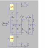
It doesn't look like a voltage doubler. It is a fullwave bridge rectification using both secondaries (18 + 18). The electrolytics are to make it possible to produce the +/- 33VDC rails with a 18-0-18 transformer.
So this can also be done with a center tapped transformer?
OK, back to basics:...
That very much higher voltage of 150% of the usual result in the regulator dissipating very much more heat.
That results in "very hot".
The heat is equivalent to power. And the power is a product of voltage and the current.
So still, nothing gets very hot...
----------------------------------------------------------------
A note for those who want to really know, not just poke in the dark with the sharp stick pretending that you know what are you talking about:
If you have a 2W part and you run 50mA through it, with 2V across it the part will dissipate 100mW and won't even feel it.
Now, increase the voltage across that part not 150%, but 300% and with the same current through it (50mA) the part will dissipate 300mW - now the 2W part will start to feel it, but it won't get even warm yet, let alone 'very hot'...
That part will become hot when it reaches a dissipation of more than 1W.
I like my amps hot. Makes them sound warm.
Juma,
Which resistors are you talking about, R1-2. The 470R that lead into the 7XXX regs?
Juma,
Which resistors are you talking about, R1-2. The 470R that lead into the 7XXX regs?
Buzz,
470R/2W resistors are running only 20mA each - the buffer draws 10mA per channel, per rail.
100R/2W resistors are running about 35mA each - the preamp draws about 17mA per channel, per rail.
When you calculate it all, have in mind that there are losses : the transformer sags a bit (it's 2x18V AC nominally), Xc of C1-C4 eats some voltage too and the rectifier bridges take their part also...
Ah. I am planning dual mono, so I was figuring half those values. Just checking. Either way, you were right and there is no excess heat anywhere.
Building a hybrid of posts #75 , #117 and #57
Hi there, I'm planning out a build using ideas from posts #75 , #117 and #57. More or less doing a LSK style frontend using J174's and one of j310/J111/j109 and lateral source followers. Attached is the basic plan of attack - although showing sk170/j74's at the moment I'd rather use the old switching jfets as a learning exercise.
My questions would be
1. what current do you guys suggest for the jfets? ie where on the curve balances best
2. which pairing would you suggest be the best, or should I just sort through for Idss and Vp and pick the closest matches?
3. where to put a pot to balance the offset at the terminals?
Of course, there are better matched parts and I didn't make an elaborate choice of these two JFETs - I just happen to have them in my parts bin.
So the scope of j175/j310 experiment was just the curiosity how will it sound (having in mind that due to cascoding only small part of transfer curve is exploited so the differences don't get the chance to become too big) and it's not bad at all...
Hi there, I'm planning out a build using ideas from posts #75 , #117 and #57. More or less doing a LSK style frontend using J174's and one of j310/J111/j109 and lateral source followers. Attached is the basic plan of attack - although showing sk170/j74's at the moment I'd rather use the old switching jfets as a learning exercise.
My questions would be
1. what current do you guys suggest for the jfets? ie where on the curve balances best
2. which pairing would you suggest be the best, or should I just sort through for Idss and Vp and pick the closest matches?
3. where to put a pot to balance the offset at the terminals?
Attachments
1. Generally, pick the most linear region on the transfer curve for the chosen JFET and try not to pair very different JFETs (like j74 and 2N3819)
2. Yes - Vp, Id, gm
3. Good places are between the sources of the input pair, between the bases of cascoding BJTs and R3/R6 on your sch. (to set LATFETs' Iq and DC offset at the amp output).
Also, there is no need to supply the LATFETs with more than +/-18V if your gain stage doesn't produce more than 15V_peak.
Thanks for the reply! I've been playing a little more in ltspice matching models of jfets and it sort of looks like a match between the J174s and the J310's looks good - Vp is quite different as does Idss but the Gm looks similar-ish (datasheet wise anyway) so I might try working through the jfets on hand for something close...
1) Wrenchone ended up at a current of about 5mA yet you seem to run higher currents through the jfets. Looking at the curves on SPICE it seems like the jfets are more linear at higher currents (or the models are a bit naff after a certain point). Do you have any suggestions from your j310 experiments?
2) I needed a good excuse to bin the parts I have anyway... 🙂
3) still considering the best spots for this - I can see the approach you took in post #118, and the the approach taken in altering the source resistance on the front end jfets (although I hadn't thought about altering the cascode reference voltage... hmm 🙂 )
Finally - yes I see your point about the latfet voltage. As it is, with the input voltage at 2V input, it swings +-15V for a 4R load. The FFT shows a lot of distortion though!
Wrenchone did much more thorough job - I just tested how it sounds when set at same Id (not bad at all)... Do you have any suggestions from your j310 experiments?
Raise the LATFETs' Id to about 1A and change the cascode voltage divider to get JFETs' Vds = 20V. Also try try raising R7 to 270R or 330R and at the same time R14 to 2k7 or 3k...... it swings +-15V for a 4R load. The FFT shows a lot of distortion though!
And don't trust sim graphs too much - many good men were driven to madness that way... 😀 Build a quick point-to-point prototype and see what you get 😉
thats the plan
Thanks again Juma - I'll sim those tweaks.
Re Building - Yup, that's the plan alright. I've the latFets on the way and it's a small and simple enough circuit that it'll be easy to knock up. Only one set of latFets though so I'll be making those connections via terminal block 🙂
And thanks for the suggestions - I'll have a play on LTSPICE and then report back after I do a build.
Cheers again!
Hi Juma, I'm playing with preamp and want to check one thing: P2 in buffer section should be used to set zero DC offset on output? If that is correct maybe R21 is a little bit to big. I have a situation where P2=0 but I still need to go lower a little bit (ok, not so much approx. 200mV). Do you think that replacing R21 with 39R or even 33R is safe and can make a difference?
Thanks once again for this great design.
Thanks once again for this great design.
Yes, P2 sets the current through CCS (Q6) in rage from 7mA to 14mA to make it equal with the current through BF862 (Q5). When the equilibrium is achieved we have 0V DC at the output.
Before we do anything else, tell me what is the voltage drop across R16 (6R8) so we can determine how much current runs through the BF862 ?
Don't forget to short-circuit the input when setting/measuring.
Before we do anything else, tell me what is the voltage drop across R16 (6R8) so we can determine how much current runs through the BF862 ?
Don't forget to short-circuit the input when setting/measuring.
- Home
- Amplifiers
- Pass Labs
- LSK pre - BAF 2013