hi guys,
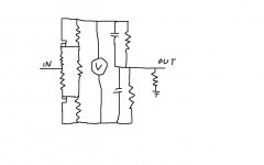
is there any reason why this topology would not work well? for a lower input impedance...
edit: maybe the circuit is not right as the gates are not reference to ground...now is bed time
is there any reason why this topology would not work well? for a lower input impedance...
edit: maybe the circuit is not right as the gates are not reference to ground...now is bed time
Attachments
Last edited:
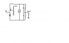
Yes, no Gnd (or Vref) reference for the gates.
See Moving Coil Cartridge Head Amps
The minute you have that Gnd reference, you have current flowing through from floating supply to Gnd.
So the two current loops are no longer totally separate.
Not the case with JFET, since no gate current, and no biasing resistor network necessary.
Patrick
See Moving Coil Cartridge Head Amps
The minute you have that Gnd reference, you have current flowing through from floating supply to Gnd.
So the two current loops are no longer totally separate.
Not the case with JFET, since no gate current, and no biasing resistor network necessary.
Patrick
Since there are so many pages, can anyone point me to the discussion (if any) to adapt the cen/sen I/V to the BII/BIIISE?
Thanks
Do
Thanks
Do
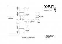
Nicmac discusses his build here:
http://www.diyaudio.com/forums/digi...minimalistic-iv-converter-62.html#post2952599
http://www.diyaudio.com/forums/digi...minimalistic-iv-converter-62.html#post2952599
Attachments

Can i still use sk117 for sen? 😀
Id be happy as long as it works
170 is hard to source in asia
Id be happy as long as it works
170 is hard to source in asia
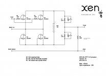
The origin of this circuit, as mentioned in the article, was Dr. Leach's MC headamp.
Moving Coil Cartridge Head Amps
The natural question arises as to whether we could use the JFET version for the same purpose.
This is being discussed independently, as I found out by chance, elsewhere :
audio-talk :: View topic - j-FET / Triode Phono front-end
(see post by JamesD on Mon Oct 07, 2013 8:26 pm)
As you would expect, we did consider this application for ourselves.
The biggest problem is DC offset.
If the Idss of the JFETs do not match and thermally track perfectly all time during operation, 2 things will occur :
1) A DC offset will be seen by the MC pickup at the input, causing a small DC current.
2) This current has to pass through R1 and/or R2, thus causing imbalance of the Vds of the two FETs.
This has been verified in Spice (I am not prepared to risk my MC pickup for that).
The second point above can be solved by replacing R2 by a Zener diode, but this does not solve the DC current problem.
To improve thermal tracking, one can :
a) use a monolithic dual JFET such as LSK389 or 2SK2145;
b) degenrate the JFET to the appropriate Zin for the MC, which also improves Id stability.
But we are trying to limit DC current to µA level, when the JFET bias is ~8mA.
In the Leach circuit, he was using 125µA bias and this was also done by a resistor network.
So there is a chance of better thermal stability.
Patrick
Patrick,
I am very enthusiastic to try the SEN IV converter. I will be using this in an OPPO-105. In this case half of the DAC lines are used for the headphone, leaving half of the Sabre DAC lines available. If I use these balanced, should I still use the suggested 16 2SK369V's for the V18 kit?
Thanks,
Eric
I am very enthusiastic to try the SEN IV converter. I will be using this in an OPPO-105. In this case half of the DAC lines are used for the headphone, leaving half of the Sabre DAC lines available. If I use these balanced, should I still use the suggested 16 2SK369V's for the V18 kit?
Thanks,
Eric
Hi
I Prove this circuit on a PCM1792, knowing that the bias current delivery. So I take the challenge. I used 2SK372 JFETs with Idss values from 16 to 17 mA. I Also used 2sk372 CCS with 20 mA Idss, with 100r pots to adjust the current to decrease the DC output voltage as possible.
To power the circuit, I utilized 2 separate regulated supplies with their own transformer (I did not use batteries) to achieve the 18 V required for each circuit. -Iout output of each channel from the PCM1792, were used.
So far it has worked great. The noise presented was minimal but, I must get close enough to the speakers to perceive it.
However, adjust repeatedly the circuit to achieve near 0 mv at the output, makes it impractical. Several post ago I read that the circuit cannot work with DC bias on the input. I made some simulations, and they confirm that the output is not consistent as one that has no DC bias on the input. However, in the simulation when changing R1 and R2 from 560k to 200r, the output becomes consistent , and by that I mean , 2 Vrms (5.6 p-p) , plus the corresponding DC bias, but can be removed later by differencial stage.
Now the question, Is this theoretically possible and thus not having to use a constant current sink, with additional PS for these (more batteries)?
Cheers
If your JFETs do not have the same Idss, they do not track each other properly thermally.
So using a trim pot for the lower FET with higher Idss is a bad idea from the DC stability's point of view.
If you want perfect tracking, then use 4x LSK389 for each single ended SEN V18.
(i.e 16x LSK389 for 2 channel balanced).
Patrick
So using a trim pot for the lower FET with higher Idss is a bad idea from the DC stability's point of view.
If you want perfect tracking, then use 4x LSK389 for each single ended SEN V18.
(i.e 16x LSK389 for 2 channel balanced).
Patrick
Last edited:
I think there was a misunderstanding. That's the general range of the JFETs used. The actual Idss of each and how were located, was:
Channel 1: upper//lower (mA)
16.64//16.68
16.71//16.68
Channel 2: upper//lower (mA)
17.08//17.11
17.14//17.11
Channel 1: upper//lower (mA)
16.64//16.68
16.71//16.68
Channel 2: upper//lower (mA)
17.08//17.11
17.14//17.11
PS
The above comment applies to DACs like PCM1704 or ES9018, which requires no offset current.
For DACs like PCM1794 requiring an offset current, we shall publish the final results of our full solution as previously mentioned in #1526 and onwards.
Patrick
The above comment applies to DACs like PCM1704 or ES9018, which requires no offset current.
For DACs like PCM1794 requiring an offset current, we shall publish the final results of our full solution as previously mentioned in #1526 and onwards.
Patrick
So 16x LSK389 substitutes 16x 2SK369V?If you want perfect tracking, then use 4x LSK389 for each single ended SEN V18.
(i.e 16x LSK389 for 2 channel balanced).
Patrick
- Home
- Source & Line
- Digital Line Level
- Zen -> Cen -> Sen, evolution of a minimalistic IV Converter