

Disconnect the dim bulb. Anything that burns I will replace. Make sure nothing lies between the FE board and the PSU. Not sure if the Soft start circuit could be responsible. Disconnect the output boards. They are not needed to make sure the FE is working. After doing the above, remeasure.
Your measurements do not make sense. At first you had a diode drop(Vbe) on the drains of the Jfet of appx. .66V. Now you have about double that.
Your measurements do not make sense. At first you had a diode drop(Vbe) on the drains of the Jfet of appx. .66V. Now you have about double that.
Last edited:
cascode bjts missing ?
As I have just bought boards and have been doing some circuit study, I was trying to understand why the BJTs were not there also... Isn't this a V3 with 47+ rails and no BJTs to cascode the FETs? Confused... I am a newb to the F5T so please enlighten me if I don't understand the obvious.
Jason
They are there. You can see them on the outer edge of the board on the top and bottom.
Thanks! The heat sinks threw me off!
SRMcGee,
What resistors are you using for your cascode with 47v rails? Your set up is similar to what I was thinking of trying.
Also for anyone, what is the ideal cascode voltage? I would imagine that it would be somewhere in the middle of the JFET parameters but I have seen anywhere from ~10V to +16V. Any benefits to either one?
Thanks!
Jason
The PCB has room to be configured many ways - deal input Jfets, parallel feedback resistors, etc... As well as extra pads on many connections, to better for more wires or different shaped resistor packages. To my eye it looks stuffed properly, as far as I can tell through the photos.
Scott - check the value of R3 and R4 - I can't tell if they are 100R or 10R. They should be 10R.
Last edited:
Regarding those extra holes.
What are those extra Jfet holes for?
In Scott's picture I think they are Q1.1 and Q2.1.
What are those extra Jfet holes for?
In Scott's picture I think they are Q1.1 and Q2.1.
In the F5 Turbo article, Nelson discussed options for making even higher powered versions. One way is to use higher rail voltages and more output device pairs. More output devices means that the front end has to drive a higher input capacitance (Ciss of the output devices). Eventually the capacitance become high enough that the amp's bandwidth is limited. Adding paralleled input devices is a way of increasing the front end's ability to drive larger output stages.
In normal use, adding doesn't buy you anything useful. If you go beyond the 4 pairs of outputs in V3, adding another (matched) input pair will help maintain your bandwidth.
In normal use, adding doesn't buy you anything useful. If you go beyond the 4 pairs of outputs in V3, adding another (matched) input pair will help maintain your bandwidth.
Folks:
The dim bulb tester is out.
Both sets of output boards have been removed and the PS is only connected to the gain stage board.
The soft start board is still in the circuit.
R3 and R4 are both 10R.
The power supply is -47.3 and +47.4 VDC.
PS ground to the drain pin on the 2sk170bl (Q1) is 0.069 VDC
PS ground to the source pin on the 2sk170bl (Q1) is 14.0 VDC
PS ground to the drain pin on the 2sj74bl (Q2) is 0.066 VDC
PS ground to the source pin on the 2sj74bl (Q2) is 14.0 VDC
PS ground to TP1 is 47.1 VDC
PS ground to TP3 is 40.8 VDC (yes, I checked it several times).
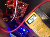
The photo shows my reading when checking PS ground to the drain on the 2sk170bl. I also checked that twice.
I am confounded. Any thoughts?
Regards,
Scott
The dim bulb tester is out.
Both sets of output boards have been removed and the PS is only connected to the gain stage board.
The soft start board is still in the circuit.
R3 and R4 are both 10R.
The power supply is -47.3 and +47.4 VDC.
PS ground to the drain pin on the 2sk170bl (Q1) is 0.069 VDC
PS ground to the source pin on the 2sk170bl (Q1) is 14.0 VDC
PS ground to the drain pin on the 2sj74bl (Q2) is 0.066 VDC
PS ground to the source pin on the 2sj74bl (Q2) is 14.0 VDC
PS ground to TP1 is 47.1 VDC
PS ground to TP3 is 40.8 VDC (yes, I checked it several times).
The photo shows my reading when checking PS ground to the drain on the 2sk170bl. I also checked that twice.
I am confounded. Any thoughts?
Regards,
Scott
Attachments
you have the jfets switched or you are measuring the wrong pins. If measuring the pins, all is good.
The pinout for the Jfets id DGS looking at the flat side.
The pinout for the Jfets id DGS looking at the flat side.
Buzz:
The jfets are in their rightful positions, so I clearly misread the datasheet. So the pins for the jfets are as follows:
S G D
____
\..../ (flat side up, curved side down)
Good to know. Nice that I managed so publicly to demonstrate that I'm a dunce.
Okay, so why was I not getting a response when diddling with P1 and P2?
Regards,
Scott
Reattach the output boards and slowly turn the pots up. Try to do both at the same time in equal amounts. The N channel will turn on first as it has lower Vgs for a given Id. Remember they are 25 turn pots.
Last edited:
Reattach the output boards and slowly turn the pots up. Try to do both at the same time in equal amounts. The N channel will turn on first as it has lower Vgs for a given Id. Remember they are 25 turn pots.
Anyone,
Is there a certain voltage that is considered "optimal" for the the LS/K170 & J74 when figuring out the resistors (R26/28) as per the BOM equation? I have seen anywhere from 10-16 volts applied in the equation to figure out the resistors. The way I think of this is you want enough to saturate but about mid-way between that and the the device break down voltage (using the J74 as the minimum). Is this accurate?
- Home
- Amplifiers
- Pass Labs
- F5 Turbo Builders Thread