Merry Christmas all with your loved ones,
May this sing in 2014....really looking forward to it 😀
Thanks for Your nice wishes🙂
 Peace
Peace Love Merry Christmas Joyeux Nöel LovePeace
I wish for All Diyaudio members keep solder station run hot and have fun
Actually, voltage is not being doubled in that PSU (post #66) - it's just the same secondary (~36V CT) being used twice (through C1-C4) to create positive and negative rail (re. to CT=GND) out of the same voltage source.
Have in mind that reactive resistance of the capacitor (Xc) is reversely proportional to its capacity and frequency of the AC voltage, so where higher current is needed use larger value caps.
Thanks for enlightment.
Didiet
On a friend's request I did a bit different version of this preamp:
- PSU voltage is lower (+/-18V)
- Gain is lower (11db, 3.5V/V)
- Zout is lower (680R) so the buffer on the output is not mandatory
- Zin is about 21k
- max. output swing is about 13V_peak
- it's an all bjt made, no need for hard to find JFETs
- current draw is about 30mA per rail, per channel
- P1 sets the DC offset which is pretty stable if the BJT pairs are thermally coupled
The most important thing: the sound is still great...
Hi JUma,
The quote is from page 11.
I am considering building this after the VSSA project that is close to completion.
2 Questions :
Are B grade 547, 557 OK ?
Which BJT pairs to thermally coupled ?
thanks and always admiring your work!
kp93300
Last edited:
Yes they are, nothing important changes drastically....Are B grade 547, 557 OK ?...
B grade has smaller hfe so the Ib will be a bit higher...
Of course, you can use BC550C/560C or similar
Those which we need to maintain the same working conditions when the temperature changes - couple Q1 to Q3 and Q2 to Q4....Which BJT pairs to thermally coupled ?...
The CCSs (Q5,Q6) dissipate about 50mW giving about 18mA each and they should be matched and coupled in order to keep delivering the same amount of current (or you can trim R5 or R8 to make them do so).
If the output offset drifts more than +/- few mV and you can't make it behave, a nice output cap (like one in BA-3) will take care of it.
You can leave out C6 an R7 if your preamp doesn't oscillate - my didn't but I put it as a precaution because most of the test builds were pretty messy...
-----------------------------
I'm writing about the circuit in the post #101 of this thread since the page number means nothing (everyone can set the number of posts per page for himself - I got 50 posts per page, so it's on page 3 for me)
Yes, by changing the degeneration and I/V conv. resistor ratio. Depending on what you want the current through corresponding active elements will need changing too....Is it possible to change the gain?
If you read the thread I think you'll find more detailed info.
Today I tested Indra1's proposal (post #76) and finally there's an amp without feedback loop that satisfies me completely (no objections to sound at all). It drives the 4 Ohm, 3-way sealed boxes magnificently.
I set the bias (R21, R22) at about 1.2A (LatFET's Vgs of about 2V).
Of course, the input stage PSU voltage should be higher, to use the full power potential of output FETs, but this was enough for the scope of the test. I used small LM317L as CCS (they do a surprisingly good job at 19mA - most thermally stable one active component CCS that I know of). DC offset at speaker is OK (+/-2.5mV). Zout is acceptable - measured at 100Hz and 10kHz it's about 0.25R
After all the tests I've done with it, I think I'm in love with this gain stage - a pity that I can't use it with VFETs due to their small gm which results in high Zout without feedback loop.
Once again, thank you Mr. Pass for bringing this great topology back to life.
Hi Juma,
we all have to thank you as well for having further developed this great topology to many different (electronic) lives.
I'd like to try the schematic as per above as a headphone amp (load 50 Ohms), eventually with reduced supply (+/- 18v) and using 2SK2013/2SJ313 as output devices (driven at 100mA). Could you kindly elaborate the changes that are needed?
Are source resistors needed?
Thanks
Guido
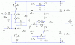
Guido, regarding the circuit in post #118 :
+/-18V for the gain stage is OK, just change R5 and R7 to 2k2. The max swing will be about 13V peak (A=9V/V) so there's no need to supply the output stage (k2013/j313) with more than +/-15V.
Before you turn it on, set the R21 and R22 to minimum resistance and short-circuit the input terminals. When you turn it on, first use the R1 to set the 0V across the R15 (R11 and C5 you can leave out if you experience no oscillations). After that, turn R21 and R22 to set the bias of the output stage and 0V at the output terminal. Do it incrementally and alternately, the same way as in F5. Let it heat up for an hour and readjust.
CCS (U1 and U2) should produce about 18mA - you can use small LM317L.
For use as a headphone amp put small source resistors on k2013/j313, about 1 Ohm.
If the gain is too high, make R15 = 1k5
Have fun !
Last edited:
FYI: I have been working on a variant of the LSK-Pre. The initial version is described in the F4 thread: http://www.diyaudio.com/forums/pass-labs/97540-f4-power-amplifier-385.html#post3684975. I am now working on adapting the LSK-pre, initially without the output buffer, to provide 40V P-P output in order to drive an F4 to full output. This requires much higher rail voltages and power dissipation for some of the components. With luck, a PCB for the LSK-Pre will be usable for the result of my adaptation.
Juma, with reference to the schematic of your attached amp, would it be possible to (1) connect the Input Gnd and junction of R8, R11 & R15 to a "Clean Gnd" (10R//Antiparallel diodes) and (2) would it be sufficient to double the rail voltages and then use a series pass regulator for higher rails for the Input Stage? By Input Stage, am I correct in understanding that it includes the entire circuit barring the Output Mosfets and associated capacitors? Many thanks.
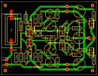
Attachments

Thank you Juma. I thought I'd add a capacitance multiplier to the darlingtion series pass regulator.
It's Iq of 1.2Amps per device?? What is the dissipation per Latfet? Thanks.
It's Iq of 1.2Amps per device?? What is the dissipation per Latfet? Thanks.
Since getting P channel JFETs is near impossible in some parts of the world, what can be done with the BJT version of the preamp for output of 20V peak?
I have some J74s but for those who may not have them, this combination of pre and power amp presented in this thread by Juma is too good to be missed!
I have some J74s but for those who may not have them, this combination of pre and power amp presented in this thread by Juma is too good to be missed!
Since it's a push-pull design, you can bias it in accordance with your needs for power ie. PSU voltage and available heatsinking. LATFETs sound good from 0.5A bias upwards - the more the better but I wouldn't go over 35W of quiescent Pd per LATFET....It's Iq of 1.2Amps per device??
Dissipated power is a product of current and voltage applied to device....What is the dissipation per Latfet?
what can be done with the BJT version of the preamp for output of 20V peak?...
It's explained earlier in the thread how to calculate the values for wanted output level. Have in mind the balance between the needed current through transistors for such a high voltage swing against the value of loading resistor. Pd_max of small BJTs could be a limiting factor (250-300mW might be needed and it's a bit too much for standard 625mW devices) so I'd use the BC639/BC640 or similar.
It's explained earlier in the thread how to calculate the values for wanted output level. Have in mind the balance between the needed current through transistors for such a high voltage swing against the value of loading resistor. Pd_max of small BJTs could be a limiting factor (250-300mW might be needed and it's a bit too much for standard 625mW devices) so I'd use the BC639/BC640 or similar.
The ON-Semi BC639/BC640 datasheets rate the power dissipation at 625mW. Fairchild rates the BC63919 at 830mW and the BC640 at 1000mW. The ON-semi BC550C/BC560C datasheets rate the power dissipation at 625mW. So which devices are you proposing for the higher voltage swing design?
Last edited:
- Home
- Amplifiers
- Pass Labs
- LSK pre - BAF 2013