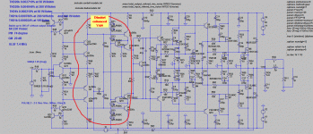
I am going to use ONE transformer for the PLUS rail and ONE for the Minus Rail...
I don't think it is good idea, I never heard that it was done before, better no, use one transformer for one mono block and other one for second mono block. No definitely not good idea.
You're right, I missed the lack of that dot connection, but the decoupling is still in the wrong place.Andrew it looks as you did not catch meaning of C10 and C11. They are cross connected between +- polarities to improve +- tracking. The C10 and C11 are in series (it is not easy to find 500u cap with 200 V rating) and parallel resistors are here to devide the voltage. The midle point is not connected to the ground.
None of those capacitors need, nor should they, be on the PSU sch.
You're right, I missed the lack of that dot connection, but the decoupling is still in the wrong place.
None of those capacitors need, nor should they, be on the PSU sch.
I don't accept that without argument.
I will use it, I have done it before, its was how I got +- 120 for my 750 watter. I use 2 Dunlap Clarke transformers and 4 per side 20Kuf caps rated at 200volts each.I don't think it is good idea, I never heard that it was done before, better no, use one transformer for one mono block and other one for second mono block. No definitely not good idea.
Have no fear. I am okay and I will be using a variac to bring them up anyway.
Attachments
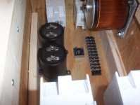
I will use it, I have done it before, its was how I got +- 120 for my 750 watter. I use 2 Dunlap Clarke transformers and 4 per side 20Kuf caps rated at 200volts each.
Have no fear. I am okay and I will be using a variac to bring them up anyway.
I have other reason not to do that. When one polarity is going down because that side of amp is in full swing then is good to have other polarity tracking it(going down too). If both polarity are comming from the same transformer then the load of it will do that tracking, not prfectly, but better then if you use separate transformers. I am not sure I know to explain that good enough in english!
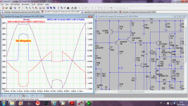
I tried here to simulate different VAS/TIS to see how much could be gained in THD, PM and GM. This is still the same 200 W CFA with lateral OPS, but with simplified compensation abd better square wave behavior.
I simulated simple one transistor VAS, EF VAS(enhanced VAS), enhanced cascode VAS, and out of curiosity Dimitri enhanced VAS. I kept the same OPS bias and type of compensation.
In my opinion I would stick with simple VAS as it gives very good distortion figure, excellent phase and gain margin, and it’s stable up to 270 nF with no output inductor, with inductor stabe on all caps value. Interesting thing is that both enhanced cascode VAS fell behind EF VAS in all parameters, and if distortion is main parameter then I would chose EF VAS.
BR Damir
Attachments
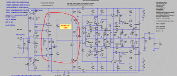
3rd version, enhanced VAS:
why is the cascode referenced to the degeneration resistor instead of to the supply rail?
Why call it "enhanced VAS"?
It looks like a cascode wrapped around the VAS? Have I missed something?
why is the cascode referenced to the degeneration resistor instead of to the supply rail?
Why call it "enhanced VAS"?
It looks like a cascode wrapped around the VAS? Have I missed something?
Last edited:
3rd version, enhanced VAS:
why is the cascode referenced to the degeneration resistor instead of to the supply rail.
This is Hawksford enhanced cascode.
Why call it "enhanced VAS"?
It looks like a cascode wrapped around the VAS? Have I missed something?
Sorry my mistake on the picture, should read enhanced cascode VAS as in the text above.
Same for 4th version picture should read Dimitri enhanced cascode VAS.
Damir
I tried here to simulate different VAS/TIS to see how much could be gained in THD, PM and GM. This is still the same 200 W CFA with lateral OPS, but with simplified compensation abd better square wave behavior.
I simulated simple one transistor VAS, EF VAS(enhanced VAS), enhanced cascode VAS, and out of curiosity Dimitri enhanced VAS. I kept the same OPS bias and type of compensation.
In my opinion I would stick with simple VAS as it gives very good distortion figure, excellent phase and gain margin, and it’s stable up to 270 nF with no output inductor, with inductor stabe on all caps value. Interesting thing is that both enhanced cascode VAS fell behind EF VAS in all parameters, and if distortion is main parameter then I would chose EF VAS.
BR Damir
Agree: during my simulations the EF VAS outperformed all my other CFA variants
2stageEF current feedback amplifier variant
Maybe you want to add some safety: a VAS current delimiter as shown in above link.
BR, Toni
Agree: during my simulations the EF VAS outperformed all my other CFA variants
2stageEF current feedback amplifier variant
Maybe you want to add some safety: a VAS current delimiter as shown in above link.
BR, Toni
Thank you Toni,
I used that kind of overload protection in my TT VFA amp, but you have to be aware that only this type of protection without EF protection collector resistor will not save EF transistor, you still need it. I think that this EF collector resistor is enough to protect against overload if big enough, look the simulations:
1. only EF collector protection resistor of 1 k, could be increased for better protection
2. EF no collector protection resistor - puff
3. protection transistor included, but no EF collector protection resistor -puff
If you want the best protection you need both type.
BR Damir
Attachments
Thank you Toni,
I used that kind of overload protection in my TT VFA amp, but you have to be aware that only this type of protection without EF protection collector resistor will not save EF transistor, you still need it. I think that this EF collector resistor is enough to protect against overload if big enough, look the simulations:
1. only EF collector protection resistor of 1 k, could be increased for better protection
2. EF no collector protection resistor - puff
3. protection transistor included, but no EF collector protection resistor -puff
If you want the best protection you need both type.
BR Damir
You a right! Every day we can learn something! 😉
Newer design of 2StageEF CFA contains a protection transistor and a 1k resistor. Interesting: This resistor is missing in many of the blameless EF VAS designs.
Br, Toni
I can confirm this is true in 'real life' too. 😡dadod said:1. only EF collector protection resistor of 1 k, could be increased for better protection
2. EF no collector protection resistor - puff
3. protection transistor included, but no EF collector protection resistor -puff
And many of these will blow up if overloaded into certain loads cos only some of the circuits in Self's book are properly protected. 😱Newer design of 2StageEF CFA contains a protection transistor and a 1k resistor. Interesting: This resistor is missing in many of the blameless EF VAS designs.
Self said he would highlight this in his latest edition. Anyone know if he did?
Last edited:
...
Self said he would highlight this in his latest edition. Anyone know if he did?
In APAD6 page 196-197.
But no overload resistor...
BR, Toni
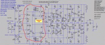
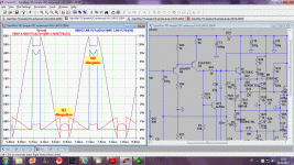
This is the Loop Gain for the amp from post #426, first schematic. I think that this is exellent result, very stable, quite low distortion and exceptionally good Phase and Gain Margins.
ULGF is quite high at 6.2 MHZ, but I think that for a CFA amp with MOSFET output it is possible to buld that amp.
BR Damir
ULGF is quite high at 6.2 MHZ, but I think that for a CFA amp with MOSFET output it is possible to buld that amp.
BR Damir
Attachments
...very stable, quite low distortion and exceptionally good Phase and Gain Margins...
Hi Damir
Looks nice, my compliments to your complements😉
As we have discussed, the outer loop is not always the critical one when there are other loops involved and exact effect of your compensation scheme is not clear to me. Some of these symmetrical layouts are a bit tricky.
Have you considered this and have any comments?
I would like to see a Tian probe between R37 and C3.
Also in the link that connects from the VAS/TIS back to the two 150p Miller compensation capacitors.
Best wishes
David
Last edited:
Ha! Guru Zan is now sneaking a peek at the other evil Loop Gain monitors that he used to spurn 😀As we have discussed, the outer loop is not always the critical one when there are other loops involved and exact effect of your compensation scheme is not clear to me. Some of these symmetrical layouts are a bit tricky.
Have you considered this and have any comments?
I would like to see a Tian probe between R37 and C3.
Also in the link that connects from the VAS/TIS back to the two 150p Miller compensation capacitors.
Damir's Tian probes in #426 are all examples of Guru Zan's Bode Return Ratio probe which Zan has in the past claimed was the ONLY stability metric worth looking at. 😱
His new requests to Damir probe the evil Outer Loop (between R37 & C3) and something that may be indeterminate or else another possibility for Bode Return Ratio around the OPS.
OK. I confess to hyperbole & putting words into Guru Zan's mouth ... and actually applaud his new, more catholic viewpoint. 🙂
Last edited:
Ha! Guru Zan is now sneaking a peek at the other evil Loop Gain monitors that he used to spurn 😀
Damir's Tian probes in #426 are all examples of Guru Zan's Bode Return Ratio probe which Zan has in the past claimed was the ONLY stability metric worth looking at. 😱
...
OK. I confess to hyperbole...
Not hyperbole but misrepresentation.
The correct place to probe depends on the circuit connection.
For pure Cherry/OIC it is in the OPS loop, as I explained.
The term "pure" is quite apt in this context because if the connection is not pure Cherry then the situation becomes more complicated.
Damir's compensation scheme has some extra components that need consideration.
I haven't analysed it in detail yet, but I don't think the outer loop is the critical determinant in his case.
Compliments and complements of the season to you too.
Need a smiley that's not only Politically Correct but season-inclusive, reindeer and snow? What about kangaroos and summer cricket😉
Best wishes
David
Last edited:
...His new requests to Damir probe the evil Outer Loop (between R37 & C3)...
Had a closer look, seems to confirm what I wrote.
It's not the outer loop, that was just curiosity.
Nor is it the loop that Damir checked, even if I expect Damir's result is probably close.
Need to probe around the VAS/TIS because of the combination of output and Miller compensation capacitors.
That looks to need a full differential probe because of the symmetrical layout both in and out.
Never actually done this, only read Dr Hurst's publications.
If Damir will post the ASC then I will post how it works out.
Best wishes
David
Dadod,
I think with MOSFET you can close the loop at much higher frequencies, but then you need to consider layout etc. As a rule of thumb, I target 3 MHz or lower for EF2 and I'd also say MOSFET because of parasitics, and 1.5 MHz for EF3. But, best is to build it and see. You can always adjust afterwards if there are problems.
I think with MOSFET you can close the loop at much higher frequencies, but then you need to consider layout etc. As a rule of thumb, I target 3 MHz or lower for EF2 and I'd also say MOSFET because of parasitics, and 1.5 MHz for EF3. But, best is to build it and see. You can always adjust afterwards if there are problems.
Had a closer look, seems to confirm what I wrote.
It's not the outer loop, that was just curiosity.
Nor is it the loop that Damir checked, even if I expect Damir's result is probably close.
Need to probe around the VAS/TIS because of the combination of output and Miller compensation capacitors.
That looks to need a full differential probe because of the symmetrical layout both in and out.
Never actually done this, only read Dr Hurst's publications.
If Damir will post the ASC then I will post how it works out.
Best wishes
David
Hi David,
Here it is, and the best wishes and happy New Year to all!
Thanks for help
Damir
Attachments
- Home
- Amplifiers
- Solid State
- 200W MOSFET CFA amp