SMD would be more commonplace these days.
You might consider it better from the point of view that the density of the pin spacing allows for complex parts to be made smaller.
However if you can get the components you need in thru-hole and are happy with the size, I would go that route as it is obviously much easier to work with.
You might consider it better from the point of view that the density of the pin spacing allows for complex parts to be made smaller.
However if you can get the components you need in thru-hole and are happy with the size, I would go that route as it is obviously much easier to work with.

SMD gets less space, and less prone to attach RFI. But are much more microfonics than through hole, some series of SMD capacitors need be retired of the market in the past for the strong piezoelectric effect that present, the much more coupling of the body with the pcb worsen the problem, the pcb acts as amplifier of vibrations.
Through hole resistors usualy distord less than SMD resistors, also are more easy find good capacitors in through hole than in SMD. And, of course, is much, much more easy work (build and repair) whit through hole than whit SMD. If no space issues I like through hole.
Sorry for my english
Through hole resistors usualy distord less than SMD resistors, also are more easy find good capacitors in through hole than in SMD. And, of course, is much, much more easy work (build and repair) whit through hole than whit SMD. If no space issues I like through hole.
Sorry for my english
Good capacitors in SMD are NP0 (for ultra-low loss, great stability) and X5R (for very high density of capacitance per unit volume, exceeding many electrolytics at lower voltages). Bad SMD caps in my experience are the electrolytics - I've found through-hole to be superior in ESR terms for same can size.
SMD resistors are something of a mixed bag - thick film are OK in lowish values when physically small, but excess noise quickly climbs at higher resistances. I tend to only use 1206 above around 10k or so. Thin film are pretty good but can easily be put out of tolerance with excess heating from soldering.
Inductors are the most difficult components to shrink of all. I've found it practically impossible to find very high Q (say above 40) in SMT and values into double digit mH are equally problematic.
I have done a few smd PCBs now.
They take me about as long as through hole to solder up.
But If I were making my own PCBs the through holes takes quite a long time to drill.
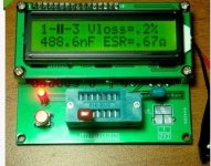
I very recently wanted to increase the RF filtering. the standard npo cap was 100pF in 805 size. I wanted 470pF, but did not have any stock.
So I used a 402 npo 330pF on top of the 805, to give 430pF.
That was very time consuming. Third attempt got it in the right place. No, it was the 4th attempt, the first one got lost on the floor. It wasn't worth getting down on my knees to try to find it. I had 49 more.
How do you stop these tiny fleas from sticking to the iron?
They take me about as long as through hole to solder up.
But If I were making my own PCBs the through holes takes quite a long time to drill.
I very recently wanted to increase the RF filtering. the standard npo cap was 100pF in 805 size. I wanted 470pF, but did not have any stock.
So I used a 402 npo 330pF on top of the 805, to give 430pF.
That was very time consuming. Third attempt got it in the right place. No, it was the 4th attempt, the first one got lost on the floor. It wasn't worth getting down on my knees to try to find it. I had 49 more.
How do you stop these tiny fleas from sticking to the iron?
I often solder on top like that to parallel values. I melt one side and I've pre-tinned the same side of the cap I'm going to solder on with a nice blob of solder. Then holding the new cap with tweezers the tinned side goes to the melted solder (the board needs holding in position mechanically here as no human hands are free). The other side can then be soldered while pressing down on the top cap with the tweezers to ensure it doesn't tombstone.
Plenty of parts get dropped on the floor here too - I also don't try to search for them.
Plenty of parts get dropped on the floor here too - I also don't try to search for them.
I saw a technique that involves pre-tinning one of the pads, hold the part down with something, then reheat the pad. Now that it is tacked, you can solder the other pins and probably go back and reflow the first "tack".
A hot air station would make life much easier. The paste idea also sounds interesting, I will look into that should I find the need to SMD.
A hot air station would make life much easier. The paste idea also sounds interesting, I will look into that should I find the need to SMD.
These have all already been mentioned, but I use SMD a lot more now because
- No need to drill holes (saves time, and makes double-sided boards easier to align).
- Lower ESL for supply bypass capacitors.
- Smaller size (allows for smaller PCBs).
If you use non-NP0 ceramic capacitors, use the physically biggest ones (1206 usually) with the highest voltage rating you can find, since they exhibit the least drop in capacitance with DC bias (the reduction in capacitance can be dramatic otherwise, but is rarely specified in the datasheet).Good capacitors in SMD are NP0 (for ultra-low loss, great stability) and X5R (for very high density of capacitance per unit volume, exceeding many electrolytics at lower voltages)...
I usually hold them down with a fingernail. Glue works too....How do you stop these tiny fleas from sticking to the iron?
I do that for ICs, but all the pads rather than just the first one. I find that I'm much less likely to accidentally bridge two pins this way.I saw a technique that involves pre-tinning one of the pads, hold the part down with something, then reheat the pad. Now that it is tacked, you can solder the other pins and probably go back and reflow the first "tack"...
If you use non-NP0 ceramic capacitors, use the physically biggest ones (1206 usually) with the highest voltage rating you can find, since they exhibit the least drop in capacitance with DC bias (the reduction in capacitance can be dramatic otherwise, but is rarely specified in the datasheet).
I've been making quite a study of X7R and X5R capacitors of late and I wonder if your remarks perhaps are based on your experience from a year or more ago? Two vendors I've found - Samsung and TDK - now do provide comprehensive data about capacitance droop against bias voltage. TDK even has a selection function which permits you to enter your bias voltage and the capacitance range you're looking for.
It turns out from looking at the graphs that its not always the highest voltage caps which do best under bias, but it usually is. I've reckon that in some cases the manufacturers probably sell (for example) the same 6.3V part labelled as 4V because I've seen plots that look identical. And yes, the drop off can be as great as 90% on the higher voltage parts (25V or more). Its also quite surprising that its not always the larger package size which gives the best performance - oddly 0805 seems to do as well as 1206 in some cases on capacitance and occasionally also with lower ESR. Certainly when both physical volume and price are taken into account, 0805 beats out 1206 handsomely most of the time, 1206 being more than twice the volume.
Many of us who have actually made the effort to learn can manually solder SMD parts down to 0805 and SOP package styles without too much difficulty. It DOES take patience, time to learn, and a modest investment in new tools.. . . Is SMD significantly "better" in some way?
For many components the parasitic effects are lower due to smaller packages and shorter leads. For audio, I doubt that the difference is very significant.
Thermal performance is a mixed bag. SMD parts are, by their nature, thermally more tightly coupled to the PWB - which can be either good or bad. Some of the SMD transistor and IC packages let you create "heatsinks" with copper on the PWB, saving the expense of a separate part, and allowing more power handling than, say, a common TO-92 or DIP8 . . . but also heating the overall PCB assembly.
And many recently designed semiconductors (as well as some long-standing types) can only be obtained in SMD packages. The BF862 JFET (high gain, low noise, decent bandwidth - although not specifically specified for audio) is a case in point.
Dale
It's good to know that more data is available now. It's been hit-and-miss in the past.I've been making quite a study of X7R and X5R capacitors of late and I wonder if your remarks perhaps are based on your experience from a year or more ago?...
Either by very awkwardly trying to use three hands to hold some probes and a fourth hand to hold the component, or by using a socket (these are typically very expensive, but more reasonably priced ones are available on eBay).How do you test SMD transistors for HFE? for matching purposes...
I would imagine direct soldering with a set of hot tweezers? HAKKO | Desoldering / Rework | HAKKO FX-8804
Ultimately so long as you don't damage the part either is fine.
Ultimately so long as you don't damage the part either is fine.

It's more likely you should put 2 and 3 together to get 23 - as in SOT-23. While there IS an SOT-22 package, the SOT-23 is more common by far.. . . did not put 2 and 2 together to get 22...
Dale
Attachments
I would imagine direct soldering with a set of hot tweezers? HAKKO | Desoldering / Rework | HAKKO FX-8804
Ultimately so long as you don't damage the part either is fine.
With Hot Air, you're stuck with solder paste, and can't use the boutique solderr....
- Home
- Design & Build
- Parts
- SMD vs through hole