First time builder question do the ztx's devices need to be matched? Also when the store offered the jfet's I ordered the A's but I should have ordered the B's is that correct?
Given a variac, what percentage of full power (120V) should I start my initial tests of my brand spankin' Aleph J at?
Should I try half power and look for 200mV across a source resistor?
Should I try half power and look for 200mV across a source resistor?
start from zero ; connect one DVM for offset , second one for Iq ( across one lower Rs)
don't be scared of funny values up to 50% mains voltage , later look at no more than double Iq ( in case of which , don't take it too long powered)
inform us what's happening
don't be scared of funny values up to 50% mains voltage , later look at no more than double Iq ( in case of which , don't take it too long powered)
inform us what's happening
slow and steady...
Thanks ZM!
I'm inspired by all the good information available on this site.
My "J" stands for Junkyard as my chassis came from the recycling outfit down the street. The heat sinks are assembled from 18 smaller computer heat sinks. The assembled heat sinks are about 14 pounds each and stand out, away and elevated from the base which itself is a tiered affair. It reminds me a bit of one of my old haunts, the Shapiro Hall of Wayne State University.
I am a few steps away, looking forward to a successful first build, taking my time... I'll post pictures if all works out
Attachments

so sad
OK...
I applied 20VAC and read 30mA across the output (binding posts) nothing across the source resistor - that seems wrong 🙁
What's more is that one side (led) of my power supply is not lit. I thought I built them identically but maybe that's the problem.
It looks pretty though 🙄
Whats a novice to do?
Attachments

Take a well-lit, in-focus photo of the PCB and let us take a look.
yeah !
and then I'll write Fugly!
😉
All I have is this image untill I tear the thing apart...
I can tell you that both LEDs have their flattened/shaved (negative) side toward the four R47 resistors and away from R9 and R10 respectively.
I'm guessing the unlit LED needs to be reversed...
What I am more concerned about (even though ZM said not to worrry about wierd numbers until half power) is the large amout of DC across the output terminals. That couldn't come from one reversed LED could it?
I've checked/traced with my finger all the connections and they all go to where they should. I'll send new pictures when I have gained access to the power supply PCB.
Attachments
new pics
Got it torn down and tried some new pics but it is darn hard to get all the leads out of the way...
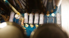
The flying leads to the rectifiers I have flagged and checked three times but that only means I did what I intended. Orientation seems appropriate to the board markings...same with the caps...the (+) mark was sometimes obscured by other markings and there is no other build of v3 I found to look at...
What do you think?
Got it torn down and tried some new pics but it is darn hard to get all the leads out of the way...
The flying leads to the rectifiers I have flagged and checked three times but that only means I did what I intended. Orientation seems appropriate to the board markings...same with the caps...the (+) mark was sometimes obscured by other markings and there is no other build of v3 I found to look at...
What do you think?
Attachments

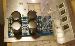
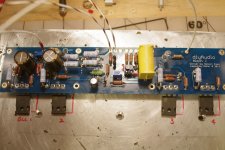
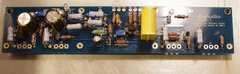
Aleph J PCBs
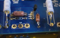
It occurred to me before I went to sleep you might want ALL PCB pics...
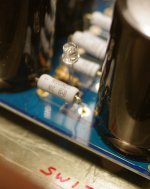
I include a close up of the orientation of the BJTs just for good measure. Besides those only the polarized caps could get screwed up. All the other LEDs light up save the one on the power board...I'll turn that one around this morning.
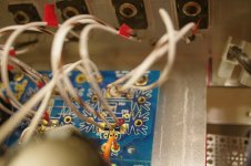
When something is screwy one should go over the basics (left off/caught between the v.3 power supply thread and the Aleph J build: both boards get a V+ and a V- from the PSU, all grounds go to the star ground, "out" goes to speaker terminal (red)-one board/speaker terminal, "in+" comes from the center pin of the RCA jack. Right?
The only thing I know I have done differently from the pictures I have found of other builds is that I took the ground wire from the RCA jack directly to the star ground. The only ground for each board is the GND1 to star ground.
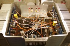
I'm thinking the above is my issue...Oh, and the wires pictured to the one Aleph J board are not soldered or the ones I used, that was a practice/dry fit, Follow the last image if possible; that's how I tested the amp.
It occurred to me before I went to sleep you might want ALL PCB pics...
I include a close up of the orientation of the BJTs just for good measure. Besides those only the polarized caps could get screwed up. All the other LEDs light up save the one on the power board...I'll turn that one around this morning.
When something is screwy one should go over the basics (left off/caught between the v.3 power supply thread and the Aleph J build: both boards get a V+ and a V- from the PSU, all grounds go to the star ground, "out" goes to speaker terminal (red)-one board/speaker terminal, "in+" comes from the center pin of the RCA jack. Right?
The only thing I know I have done differently from the pictures I have found of other builds is that I took the ground wire from the RCA jack directly to the star ground. The only ground for each board is the GND1 to star ground.
I'm thinking the above is my issue...Oh, and the wires pictured to the one Aleph J board are not soldered or the ones I used, that was a practice/dry fit, Follow the last image if possible; that's how I tested the amp.
Attachments
Hello again,
I turned around that LED for the V- boad and it's lit now. I changed the grounding of the RCA input to the board.
I got the same results when I tested the DC offset at 20VAC in. I bumped it up to 25VAC in and read 190mA across the speaker terminals
I thought I did a good job populating the boards. I set the initials for R27 at 68K and R7 at 1K. Everything looks right to me. Can anyone help?
I can't see it well on the pictures, but is -IN grounded? Is there on R2 a 2213 or 2210 marking?
Walter
Walter
Hello again,
I turned around that LED for the V- boad and it's lit now. I changed the grounding of the RCA input to the board.
I got the same results when I tested the DC offset at 20VAC in. I bumped it up to 25VAC in and read 190mA across the speaker terminals
I thought I did a good job populating the boards. I set the initials for R27 at 68K and R7 at 1K. Everything looks right to me. Can anyone help?
Why are you changing your VAC ? And I guess you mean 190 mV across the speaker terminals?
Walter
2213 is ok, you should ground -IN, though it wouldn't have much to do with bias and offset...
Walter
Walter
I have not had the heart to do even a half power attempt as bringing up the VAC from zero to 20V brought on this large DC offset across the speaker terminals. At 25VAC I got 190mA across the speaker terminals...
I will ground -IN
I will ground -IN
I have to go away for the weekend now. I'll worry about it, take my data, see if I can find anything. Thanks to all who have tried to help. Maybe it is just a thing with the very low power I am applying?
Please use your big "ol brains on this guys, I'm so sad and so confused. I want to do a good job...
Please use your big "ol brains on this guys, I'm so sad and so confused. I want to do a good job...
- Home
- Amplifiers
- Pass Labs
- Aleph J illustrated build guide