Yes. My discrete darlington version hasn't seen the real life...
I have had a quick look at your initial outline and I think it can be optimised to do even better than the conventional version.
But only if you call it a "distributed driver"😉
That is a more accurate description, not just my hobby-horse.
Best wishes
David
IBut only if you call it a "distributed driver"😉
That is a more accurate description
I concur.
Dave, have you considered using a cascode output stage? A long while ago in a different thread I mentioned some very fast high current rated devices from Sanyo, but they have limited SOA so it wasn't clear how easy it would be to use them. Sanyo/ON-Semi have launched some new transistors that look at lot more promising.
Check out the 2SC6144SG and 2SA2222SG. Rated at 50 V/10 A, beta is nice and flat and doesn't droop until about 5 A, Ft is in excess of 100 MHz from 70 mA to 7 A, and Cob is small. As already alluded to, voltage rating and SOA means these would have to be cascoded with MJL4xxx devices.
I have ordered some from Mouser. The NPN part is already in stock but the PNP part has a longish leadtime. My order means that Mouser should have stock in about 6 months from now.
Of course we can call it "distributed driver" if it describes the topology better. 😉I have had a quick look at your initial outline and I think it can be optimised to do even better than the conventional version.
But only if you call it a "distributed driver"😉
That is a more accurate description, not just my hobby-horse.
Best wishes
David
Hope we soon can get a first look on an optimized version of asc file from post #278 ...
BR, Toni
I concur.
Dave, have you considered ... a cascode output...
Check out the 2SC6144SG and 2SA2222SG. Rated at 50 V/10 A, beta is nice and flat and doesn't droop until about 5 A, Ft is in excess of 100 MHz from 70 mA to 7 A, and Cob is small. As already alluded to, voltage rating and SOA means these would have to be cascoded with MJL4xxx devices.
Thanks for the concurrence and information.
I haven't really considered cascode outputs seriously yet, so many possibilities.
So far I have focused on improvements to compensation and other areas.
Those transistors look impressive but NJL4xxx are already pretty flat and fast, >50MHz peak.
Probably sufficient for <0.001% distortion at full power.
Toni is already close to that and I have decided I need to have a cut off point, and that's it.
Best wishes
David
Hope we soon can get a first look on an optimized version of asc file from post #278 ...
Hi Toni. I have started to play around with this and tried to optimise the conventional version first.
I am not sure that I have an up to date ASC for your current version, you may have altered a few values already.
But for the version I have I found that the VAS emitter resistor bypass capacitor should about 12nF.
There should be no series resistor with the capacitor.
The 470pF TMC capacitor should be reduced to 220pF and the TMC resistor to 220 ohms.
You may want to simulate this, I found it effective.
Best wishes
David
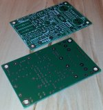
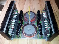
Looks nice, as usual.
I just noticed, how many layers on that board?
Last edited:
Thanks!...
Looks nice, as usual.
I just noticed, how many layers on that board?
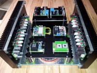
Board is using 2 layers - the bottom side is mostly signal ground and partially power ground.
Gerber files will follow soon if RC1 is stable.
Attached an up2date version using distributed drivers.
BR, Toni
Attachments
Attached an up2date version using distributed drivers.
What I meant was to try a simulation with those values in your conventional version.
I found an improvement in stability and should be lower distortion too.
I studied the non-minimum-phase from the zero and came up with improved values I think.
Thanks for the ASC.
The solder mask on the boards does not show the traces and I wondered if you had just a plane on each side and a 4 layer board.
I have never tried a 4 layer layout and want to learn more.
Best wishes
David
Last edited:
What I meant was to try a simulation with those values in your conventional version.
...
Sorry. Here we are ...
Attachments
...
But for the version I have I found that the VAS emitter resistor bypass capacitor should about 12nF.
There should be no series resistor with the capacitor.
The 470pF TMC capacitor should be reduced to 220pF and the TMC resistor to 220 ohms.
You may want to simulate this, I found it effective.
Dear Dave,
using current asc file and upper values the PM looks good - about 63 degree.
But GM is < 9dB. Maybe too less GM?
BR, Toni
Dear Dave,
using current asc file and upper values the PM looks good - about 63 degree.
But GM is < 9dB. Maybe too less GM?
BR, Toni
Yes I wondered about that, but I think it's fine.
Cordell says at least 6 and he is sensible.
Nichols plot shows approximate trade off of GM and PM and 9dB is plenty.
Best wishes
David
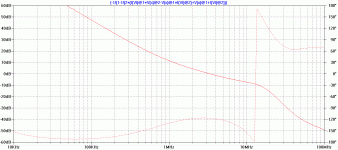
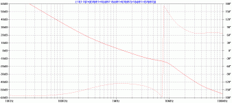
Dave, 609.gif & 609nyq.gif are Loop Gain for Toni's #609 circuit as is. Good margins and Nyquist keeps well away from (-1,0)
609Z.gif & 609Znyq.gif have your recommendations that Toni lists in #610 including the 12n across R22, the VAS emitter resistor.
I think his #609 circuit is a better compromise as the distance from (-1,0) is large and fairly constant.
Your version has better PM (the distance when Loop Gain cuts the unit circle) at the expense of GM (the distance where LG crosses the Re axis)
I haven't done any THD or stability with other loads.
Have you worked out how to do Nichols in LTspice?Nichols plot shows approximate trade off of GM and PM and 9dB is plenty.
Attachments

Last edited:
Your version has better PM (the distance when Loop Gain cuts the unit circle) at the expense of GM (the distance where LG crosses the Re axis)
I haven't done any THD or stability with other loads.
Have you worked out how to do Nichols in LTspice?
Bode optimisation trades a little loss of GM for improved PM.
The point is that I have stability that is similar (or a little better maybe) but with double the feedback so should be about half the distortion.
Can't see how to do Nichols plot in Spice yet. I use the Nichols chart to compare PM with GM to optimise trade-off
More later. Have nice Toshiba low noise monolithic pair transistors to collect from post office😉
Best wishes
David
Ok. The explanation.
I don't think we need to worry too much about circuit variability.
A proper compensation scheme will set the relevant return ratio with well defined passive components rather than unpredictable transistor parameters. 1% metal film resistors and 5% capacitors or better, probably.
So we can optimise the feedback network for best response at nominal.
We eliminate all the RHP zeros so essentially no excess phase (used strictly).
That means the frequency response is all we need to consider because it essentially defines the behaviour.
For instance the impulse response is just a transformation and will be nice if the frequency response is smooth.
The Nichols chart shows how much response peak occurs for various combinations of phase and gain difference. One curve intersects about 60 degrees (one radian) and 6 dB. So that is a balanced trade-off.
I have a bit more than 60 degrees of PM and about 9dB of GM.
Actually a bit conservative on GM.
And the new values have a little better PM and about double the return ratio.
THD should be better but I haven't simulated it yet, the smaller resistor and smaller capacitor is a closer approximation to "pure" Cherry so I expected you would want to.😉
Best wishes
David
.
Last edited:
I do Dave. The better Loop Gain is the reason I've been looking for.THD should be better but I haven't simulated it yet, the smaller resistor and smaller capacitor is a closer approximation to "pure" Cherry so I expected you would want to.😉
But I have to do a fair amount of editing of Toni's .ASC to run the THD analyzer.
Alas I'm still trying to recover files and my email capability. I'm only posting here when I need to do something which will prevent me from hurling the computer into the sea. 😱
But I have to do a fair amount of editing of Toni's .ASC to run the THD analyzer.
Yes. I wanted to tidy it up a little too, so I know what is there and don't overlook some hidden detail. That's why I asked Toni to try my values.
Best of luck with your recovery and thanks for the low noise data.
Best wishes
David
Yes. I wanted to tidy it up a little too, so I know what is there and don't overlook some hidden detail. That's why I asked Toni to try my values.
...
Dear David,
just tried your values but amplifier is not stable and starts oscillation at about 6 to 7 Mhz. Short or long ribbon cable has nearly no influence.
Tested TMC values where:
- 470R => 220R
- 470p => 220p
- 12nF cap parallel to VAS emitter resistor
Think we have reached the limits of this design. Maybe a small change of the pcb layout and/or cabling would help to get below 10ppm THD20k@200W@8R.
The next days I will assemble the Rev. 2.0-RC1 pcb's and make some measurements.
BR, Toni

- Home
- Amplifiers
- Solid State
- 2stageEF high performance class AB power amp / 200W8R / 400W4R