ah, ok, sorry
it was just the 'not that Im aware of' I reacted to
so, mixing them may still prove 'tricky'....and problematic for most of us ?
and if not knowing what kind of solder have been used ....maybe even more ?
so, what is worst ?
adding lead free to lead solder ?
or adding lead solder to lead free ?
not the same thing, is it ?
ah, ok, sorry
it was just the 'not that Im aware of' I reacted to
so, mixing them may still prove 'tricky'....and problematic for most of us ?
and if not knowing what kind of solder have been used ....maybe even more ?
so, what is worst ?
adding lead free to lead solder ?
or adding lead solder to lead free ?
not the same thing, is it ?
I have had the easier time putting lead into lead free. It lowers the melt temp, easier on the flux. It'll never look pretty because you won't go eutectic unless you wick out the excess to replace. But the flux will generally make the stuff give a reasonable joint.
If the stuff is soldered, why drop lead into it? I haven't read of tin whiskers for eutectic tin/silver yet. I do feel swamping out pure tin plating is needed however.
I'd never use tin silver to rework a part though...always tin/lead.
jn
Its a colloquial phrase over here in the UK.
Not a problem for commercial gear, but for mission/life critical and long term reliability its a major concern.
Empfasis - Ask the EMPF Helpline
Can You Mix Leaded and Lead-free?
High reliability, got to use lead based solder, didn't get good joints on the BGA's, long term reliability and greater possibility of cracks with elevated temperature range. No free ride though as unless you use laser re-balling your device is subjected to a thermal cycle, and again these had to be limited, preferably to 2 max. Smaller components OK, though again a tin/lead finish was chosen if available, or components re-tinned with tin/lead.If you have replaced BGA balls with tin/lead, I assume you've done so with other components? Or are you trying to mix tin/lead BGA soldering with external component lead free through the same wave or IR?
Not a problem for commercial gear, but for mission/life critical and long term reliability its a major concern.
Empfasis - Ask the EMPF Helpline
Can You Mix Leaded and Lead-free?
http://www.hlinstruments.com/RoHS_articles/Tin whiskers from tin alloy coatings.pdf
As far as I know the only way to stop whiskers is 3% or greater lead added to the mix.
As far as I know the only way to stop whiskers is 3% or greater lead added to the mix.
Its a colloquial phrase over here in the UK.
Ah, got it. We say pencil lead here as well, but no actual Pb..
I had to "convince" upper management here that banning tin/lead was an idea worse than launching a shuttle in 28 degree weather. We designed and farmed out over 8 thousand large dense surface mount boards, and "insisted" that they all be tin/lead. Also that tin plating had to go away. When the work was let, two thirds of all components were already pure tin plated.High reliability, got to use lead based solder, didn't get good joints on the BGA's, long term reliability and greater possibility of cracks with elevated temperature range. No free ride though as unless you use laser re-balling your device is subjected to a thermal cycle, and again these had to be limited, preferably to 2 max. Smaller components OK, though again a tin/lead finish was chosen if available, or components re-tinned with tin/lead.
Not a problem for commercial gear, but for mission/life critical and long term reliability its a major concern.
I recall reading something to that effect years ago. But I also recall that there was insufficient data to say if silver also did the same back then. My tin/silver work unfortunately, clears whiskers if they develop, as the application supports some very significant currents. So I cannot claim it a solution.http://www.hlinstruments.com/RoHS_articles/Tin whiskers from tin alloy coatings.pdf
As far as I know the only way to stop whiskers is 3% or greater lead added to the mix.
ps...your link didn't work for me, but I suspect it's on my end. Web's been acting up today.
jn
Last edited:
Hence all the ridiculous amounts of flux.😛Um, I speak from experience.
The hardest part is getting a flux which activates below 150C and remains unburned above 260 C.
I will say that with all of my distaste for lead free solder for electronic works I did manage to construct THIS
prototype by hand, soldering each and every pin including the 0402X4😀 resistor arrays using 22mil 99.2Sn/0.3Ag/0.5Cu lead free solder from RS. That proto still works wonderfully. I will say that particular blend of solder IS harder to work with than 60/40 but managable. Next build on this level will be done with 60/40.
Had a look at your design CBS240, one question, why when you have used SMD have you spread them out so much? It is not just your design but other SMD designs on here, they regularly spread the devices out.
Had a look at your design CBS240, one question, why when you have used SMD have you spread them out so much? It is not just your design but other SMD designs on here, they regularly spread the devices out.
Sigh...they don't do that here. The tradeoff is number of layers.
Honestly, some of the boards have the look and feel of 60 grit sandpaper. It's hard to imagine a schematic which requires so many caps and resistors..
I truly like power devices, something I don't need a microscope to see.
jn
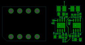
Spacing between SMD lands may be to allow old fashioned hand soldering methods to gain access to the individual solder pads.
Yes. When creating a prototype PCB it becomes necessary to change component values as you troubleshoot each circuit so reflow is out. If your design is accurate you won't have too much trouble barring a steady hand and a magnifying glass.😛 Spacing would be for 3 reasons, 1) the PCB is only 2 layers and the space is needed for routing. 2) heat dissipation. With SMDs the PCB and the copper pads are the heat sink. 3) Hi current routing takes precedence in placement with small signal and control circuits of lesser importance. I like grouping the components of one of the many circuits together in a general area.
All the footprints are to the IPC-7351 standard (least). The actual full board is a 8 layer HDI construction. The smallest devices are 0201 chip devices, and some people can re-work them. I'm not one of them, most of what I layout is just a blur these days.Spacing between SMD lands may be to allow old fashioned hand soldering methods to gain access to the individual solder pads.
Most of the routing is shown, on the top layer, the vias shown are laser drilled 0.1mm hole, 0.3mm pad.
A bit extreme for DIY. Add this headphone amp (the bga package) and you have a very very small headphone amp, think small portable devices.
Oh and don't forget
tin-bismuth-silver solder
a new one just announced has less than 1% silver for improved mechanical resilience, lower temperatures as well, though again not without its problems, as setting an optimum profile becomes more critical.
tin-bismuth-silver solder
a new one just announced has less than 1% silver for improved mechanical resilience, lower temperatures as well, though again not without its problems, as setting an optimum profile becomes more critical.
All the footprints are to the IPC-7351 standard (least). The actual full board is a 8 layer HDI construction. The smallest devices are 0201 chip devices, and some people can re-work them. I'm not one of them, most of what I layout is just a blur these days.
Most of the routing is shown, on the top layer, the vias shown are laser drilled 0.1mm hole, 0.3mm pad.
A bit extreme for DIY. Add this headphone amp (the bga package) and you have a very very small headphone amp, think small portable devices.
I use 0201 resistors in that project I posted, several 0201 resistors in fact. None of them are running above 40% of the 0201 de-rated Pd rating. I can hand solder them, but it is not as easy as 0402 size. It takes a certain technique. 😛 SOT-923 is quite small as well.
 That PCB includes the complete power supply along with all the logic and protection circuitry which is why it looks so complex with so many parts.
 They are not just thrown in for sh!ts & giggles. There is a half dozen different seperate circuits on that PCB. The PCB is only 2 layers, 1 Oz Cu. Vias are 10mil. All cut-outs were done by me, it cost a lot extra to have the boardhouse make cut-outs. Overall, I paid ~$100 for 5 PCBs including shipping.
Last edited:

Oh and don't forget
tin-bismuth-silver solder
a new one just announced has less than 1% silver for improved mechanical resilience, lower temperatures as well, though again not without its problems, as setting an optimum profile becomes more critical.
Uh, bismuth again..
IBM (it may have been Bell labs actually, it was a top of the pole application, so I'm thinking telephone electronics. Read about it back in '85, so memory's fuzzy
 ) had a wave setup with bismuth loaded solder. The advantage was very little density change during the liquid to solid transition. As a consequence, there was far less shear stress built into the joints than would normally occur with tin/lead.
This was done to reduce the low cycle fatigue problem experienced by electronics in the outdoor environment. The 24 hour temp cycle caused by outdoor use caused the lead/tin joints to fail prematurely. The slow temp cycle allowed ductile creep, and that worked the grain boundaries of the solder.
Bismuth was an attempted solution. AFAIK, it did not continue long. Apparently, they decided to concentrate on joint design to reduce stress.
jn
Last edited:
And again
Its coming back into fashion, there been a flurry of recent articles and news blogs in the PCB and Assembly press (well a couple, flurry is possibly an exaggeration🙂)
If we are lucky we'll circle back to good old tin/lead.
New! Tin Bismuth Wire Solder, Sn42/Bi58 Alloy, Low Melting Point Lead Free Wire Solder
Printed Circuit Design & Fab Magazine Online
http://www.ipcoutlook.org/pdf/manufacturability_reliability_screening_ipc.pdf
And again
Its coming back into fashion, there been a flurry of recent articles and news blogs in the PCB and Assembly press (well a couple, flurry is possibly an exaggeration🙂)
If we are lucky we'll circle back to good old tin/lead.
New! Tin Bismuth Wire Solder, Sn42/Bi58 Alloy, Low Melting Point Lead Free Wire Solder
Printed Circuit Design & Fab Magazine Online
http://www.ipcoutlook.org/pdf/manufacturability_reliability_screening_ipc.pdf
Nice links. I was reading the third one when it caved..Now, the link gets me an error saying the document is broken.
It must be Ed's fault (simon7000).
jn
- Status
- Not open for further replies.
- Home
- Design & Build
- Parts
- Leaded or unleaded solder ?