So anyone wants to take on the challenge to redo the layout in post #1379 using a PCB layout software ?
Schematics is here :
http://www.diyaudio.com/forums/anal...discrete-opamp-open-design-3.html#post3138073
Footprint is 10x10mm, DIP8 single opamp pin out for Pins 2,3,4,6,7.
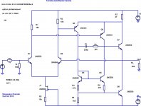
I will eventually do a BJT Kaneda variant, similar to the schematic shown below. It will however be larger than 10x10, even with SMDs, because it has 9 actives. No schedule or timeline at the moment.
Attachments
Last edited:
Anyone who has seen the F5X PCB and is intimately familiar with PCB layout tools from ten years or so ago will understand the reason for the time it took. The original layout he did was as much art as function. No corners at all, very few parallel edges of copper areas, and few if any simple, straight traces. Everything was curves and freehand copper area to match Patrick's desired esthetic and other design goals of his own. Grids, what grids? I agreed to duplicate the original from Patrick’s dxf artwork in a PCB tool package so that it was maintainable. Good news is that it worked first time out of the gate, no changes necessary. The finished product has the addition of the cascode options while staying extremely close to the original.
The software used for the F5X layout has a lot in common with other layout tools I’m familiar with. Like others it supports creating any arbitrary shape you like in a copper area for any net. It is a lot of extra work in that every copper shape on this design was not an trace and so had to be hand defined as a plane for the net, side, type, etc. manually.
And like some other layout software this one thinks in polygons or traces only. There is no free handing it with the tool I used. Any arcs in the copper shapes were limited to the amount of manipulation that could be done to rounded corners with limits imposed by the tools geometric minimums. Every conductor shape was composed of many complex arcs so needless to say it was a challenge. In the end it is so close you probably would not know unless you held them up to one another…
Layouts consisting mostly of traces and simple polygon shapes are no problem in modern layout tools.
Dave
yeah, my first attemps at doing some PCBs for myself have been in Adobe illustrator, which I know very well, but I would love to be able to transfer to Maya to allow full visualization in 3D. nice to know i'm not the only one doing it this way. isnt there plugins for autocad to allow direct printing of PCBs via CNC?
> I don't use any 8 pin DIP opamps
I do, as most others here, and elsewhere.
> I may have to lay one out for myself.
I think it is always wise to do so.
Patrick
I do, as most others here, and elsewhere.
> I may have to lay one out for myself.
I think it is always wise to do so.
Patrick
> It will however be larger than 10x10, even with SMDs, because it has 9 actives.
I have done 7x SOT23 on a 10x10 DIP8 before.
These days there are more choices with dual devices in SOT23.
So you pack 2 transistors into the same foot print.
There might still be a chance to do it in 10x10.
This one is half BJT, half FETs. And not quite 10x10. But still DIP8.
mic???????? OP???
Good luck,
Patrick
Unfortunately, there does appear to be some "issue" here with the sensitivity of the DC output level to the source resistors. I took dadod's version of circuit, and considered the "worst" arrangement of 1% resistors, which means +-1%, an effective 2% range, 24.75R and 25.25R
Used FB of R18=670, R19=67k and inter source resistor R5=250. For R1=R4=25.25, R2=R3=24.75, DC Op Point was -222mV; for R1=R4=24.75, R2=R3=25.25, DC Op Point was 497mV. Reducing R5 back to 50R only improved things slightly, 497mV to 402mV ...
Frank
Used FB of R18=670, R19=67k and inter source resistor R5=250. For R1=R4=25.25, R2=R3=24.75, DC Op Point was -222mV; for R1=R4=24.75, R2=R3=25.25, DC Op Point was 497mV. Reducing R5 back to 50R only improved things slightly, 497mV to 402mV ...
Frank
EOL announced for the 2SJ144 🙁
2SJ144?Junction FETs?TOSHIBA Semiconductor & Storage Products Company
That is a lot of gain though (x101 I presume, not looking at the schematic but supposing that 67k is feedback and 670 feedback divider).Unfortunately, there does appear to be some "issue" here with the sensitivity of the DC output level to the source resistors. I took dadod's version of circuit, and considered the "worst" arrangement of 1% resistors, which means +-1%, an effective 2% range, 24.75R and 25.25R
Used FB of R18=670, R19=67k and inter source resistor R5=250. For R1=R4=25.25, R2=R3=24.75, DC Op Point was -222mV; for R1=R4=24.75, R2=R3=25.25, DC Op Point was 497mV. Reducing R5 back to 50R only improved things slightly, 497mV to 402mV ...
Frank
It's easy to source 0.1% resistors. But at that, unless the input devices are well-matched duals, their mismatch is likely to dominate.
If one is attempting to take on the good IC devices, then the Input Offset Voltage, which is what we're talking about here, needs to be of the same order. Those figures, yes, x101 gain, translate to 5mV offset, and that's purely because of the source resistors, mismatch of the actives could possibly make it worse. For comparison, the LM4562 does 0.1mV offset, typically ...
Frank
Frank
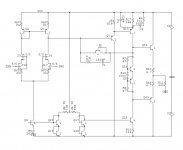
Here's a first shot at a FET input JE990 for 600 Ohm type loads. This was easier than I thought, almost the same values worked with minor changes and the performance was virtually identicle to the original. Most importantly the noise is just slightly higher, but still well below 2nV.
Notes
Input FET's are BF862, 2SK170, LSK389, etc. cascoded by J111 or J305 depending on voltage range. Personally I think it is easy to select for +-18V or +-24V from actual FET's but +-15V will always work. Even a 100k input R is OK now.
I used 2SA970 and 2SC2240 in all locations, later I will try to do a high current version.
C1 is the comp cap, this can be reduced to suit the closed loop gain, a big advantage in having access to the whole circuit.
R10 (5k pot) selects the standing current in the output stage, I find this essential because trying to match diodes to transistor Vbe's is silly.
The first thing I would change is to use a current source to generate bias and provide for an offst trim in the current mirror.
I think this would do well up against an OPA627/37.
EDIT - No inductors needed.
Attachments
Here's a first shot at a FET input JE990 for 600 Ohm type loads. This was easier than I thought, almost the same values worked with minor changes and the performance was virtually identicle to the original. Most importantly the noise is just slightly higher, but still well below 2nV.
Notes
Input FET's are BF862, 2SK170, LSK389, etc. cascoded by J111 or J305 depending on voltage range. Personally I think it is easy to select for +-18V or +-24V from actual FET's but +-15V will always work. Even a 100k input R is OK now.
I used 2SA970 and 2SC2240 in all locations, later I will try to do a high current version.
C1 is the comp cap, this can be reduced to suit the closed loop gain, a big advantage in having access to the whole circuit.
R10 (5k pot) selects the standing current in the output stage, I find this essential because trying to match diodes to transistor Vbe's is silly.
The first thing I would change is to use a current source to generate bias and provide for an offst trim in the current mirror.
I think this would do well up against an OPA627/37.
EDIT - No inductors needed.
I suggest to use deplation mode mosfets from Supertex for J3, J4, DN2540 could be good for it, more voltage for input fets.
dado
dadod, I downloaded your LTSpice script but it won't run. Keeps asking for supertex.txtI suggest to use deplation mode mosfets from Supertex for J3, J4, DN2540 could be good for it, more voltage for input fets
Can you post a copy or give a link to this please.
dadod, I downloaded your LTSpice script but it won't run. Keeps asking for supertex.txt
Can you post a copy or give a link to this please.
Just remove the line .include supertex.txt, you don't need it as in the simulation no supertex fet was used.
dadod, i think it is J1, J3 where you would put the depletion mosfets.
Depends what schematic you are looking at, Wurcer (J3, J4) or fas42 (J1, J3), of course upper cascode fets.
Hello Scott, just one question.
Did you put the Q3(in your schematic), connected as a diode, intentionally to get higher secon harmonic distortion(as benign one)? My simulation shows that distortion was more than halved if that diode was not connected parallel to the compensation RC, and at that only second harmonic.
Damir
Did you put the Q3(in your schematic), connected as a diode, intentionally to get higher secon harmonic distortion(as benign one)? My simulation shows that distortion was more than halved if that diode was not connected parallel to the compensation RC, and at that only second harmonic.
Damir
Attachments
Hello Scott, just one question.
Did you put the Q3(in your schematic), connected as a diode, intentionally to get higher secon harmonic distortion(as benign one)? My simulation shows that distortion was more than halved if that diode was not connected parallel to the compensation RC, and at that only second harmonic.
Damir
JE990 had that as a clamp? just Muntz it.😀
As before the diode connected transistors could just be diodes, just my habit because we usually don't have diodes per se in an IC. A very low C discrete diode here probably would not have the problem as much (in case the clamp is really needed). The worst latch-up tests are usually power on with signal already applied, this always violates the data sheet since with power off and any input signal you are exceeding the supply on the input.
Also I left the "fiddly" compensation components as is, with different devices you may want to revisit them.
Last edited:
Or possibly DN1509, a 90V part with lower capacitances, about the same threshold voltages. It seems somewhat less characterized than the older parts as the datasheet lacks curves.I suggest to use deplation mode mosfets from Supertex for J3, J4, DN2540 could be good for it, more voltage for input fets.
dado
Or possibly DN1509, a 90V part with lower capacitances, about the same threshold voltages. It seems somewhat less characterized than the older parts as the datasheet lacks curves.
How about CPC3730 from C P Clare? With that and some 140V transistors this could be the front end of a 100W amp.
Last edited:
- Home
- Source & Line
- Analog Line Level
- Discrete Opamp Open Design