I built this and it works
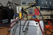
Here is my guess at the F6 design, built with Semisouth R100s and the Jensen JT-123-FLPCH transformer.
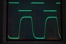
The first scope photo shows response to a 20kHz square wave.
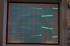
The second scope photo shows response to a 20Hz square wave.
In both cases, the top trace is the input after the input coupling capacitor and the F6 bottom is the output.
Posts 890 and 902 show THD measurements. Ignore the frequency sweep in post 890, it is corrected in post 902.
The R100 bias currents and output offset voltage are rock-solid stable. The positive temperature of the R100 means that thermistors are not needed for temperature stabilization. When cold, the bias currents start slightly higher than when at final running temperature.
I do not know how well this performs vs. Nelson's "official F6".
I haven't listened to it yet. I first plan build a second channel for stereo.
Here is my guess at the F6 design, built with Semisouth R100s and the Jensen JT-123-FLPCH transformer.
The first scope photo shows response to a 20kHz square wave.
The second scope photo shows response to a 20Hz square wave.
In both cases, the top trace is the input after the input coupling capacitor and the F6 bottom is the output.
Posts 890 and 902 show THD measurements. Ignore the frequency sweep in post 890, it is corrected in post 902.
The R100 bias currents and output offset voltage are rock-solid stable. The positive temperature of the R100 means that thermistors are not needed for temperature stabilization. When cold, the bias currents start slightly higher than when at final running temperature.
I do not know how well this performs vs. Nelson's "official F6".
I haven't listened to it yet. I first plan build a second channel for stereo.
Attachments
Last edited:
Thank you banat. I got it. Is the underlined saying thats the AC mains power plug [or maybe the mains power transformer] to Conceptual F6 needs to to be inserted/wired one way only, and not the other for maximizing PSSR?. This is an unexpeted find.Antoinel
Here is the link to DIY Atma-Sphere M60 OTL Circlotron tube amp , there you can find the schematic ,altogether with many valuable blah - blah stuff , ( including mine blah - blah stuff ) : http://www.diyaudio.com/forums/tubes-valves/161112-what-tubes-tube-amp-2.html
BTW , if you want to make bias network for F6 Amp in the same way as is done on SEPP OTL Tube amp from mine previous attached schematic than .....
It is just my personal opinion that is important thing to succesfully DIY F6 SS SEPP amp to find Right relative main ( 60 Hz) AC phase status between this two equal independent & floating bias secondary coils on main PSU transf.
By reversing relative AC phase of this two independent secondary bias coils you can worse or improve Amp output power stage (SEPP) PSRR significantly .
Same is valuable for relative relation between output power stage (SEPP) PSU secondary power coil AC main phase and this two independent bias coils AC phases .
Best Regards !
Best regards.
The first scope photo shows response to a 20kHz square wave. The second scope photo shows response to a 20Hz square wave. In both cases, the top trace is the input after the input coupling capacitor and the F6 bottom is the output.
Why is the output inverted with respect to the input?
Here is my guess at the F6......
upper half bias doesn't need to go to gnd , but output rail
besides that , try to implement "those" few things in second iteration , then hear and measure difference
Oops, my mistake. I inadvertently had the bottom scope channel invert switch depressed. I had been using it to do a differential voltage measurement and forgot to switch it off.Why is the output inverted with respect to the input?
When connected to the amplifier output the offset voltage would not stabilize. When it is connected to ground it is totally stable.upper half bias doesn't need to go to gnd , but output rail
besides that , try to implement "those" few things in second iteration , then hear and measure difference
My theory is the following:
- Let X be the bottom connection of the upper bias circuit.
- The capacitor C5 from the secondary to the gate stopper resistor integrates the current supplied thru the bias injection resistor R12. The voltage across C5 should be the offset voltage of the bias circuit plus the average voltage of X.
- The average value of the output should be zero. Therefore we can connect X to ground.
- This seems to work well, but depends on the RC time constant of C5 and R12 being large enough. However, spice simulations show better results at low power levels with X connected to the output.
sorry
I neglected that you're having fixed voltage across LED's (unlike as in case of using just resistors)
in this case is certainly better as you drew it
I neglected that you're having fixed voltage across LED's (unlike as in case of using just resistors)
in this case is certainly better as you drew it
Thank you banat. I got it. Is the underlined saying thats the AC mains power plug [or maybe the mains power transformer] to Conceptual F6 needs to to be inserted/wired one way only, and not the other for maximizing PSSR?. This is an unexpeted find.
Best regards.
If the F6 both bias DC sources is done in Unregulated way same as is done on that SEPP OTL tube amp schematic than is important to take care of the mutual phase relation between this three PSU transf. secondaries , regardless if that three secondary coils is on the common main power transf. or not ,
since the some minor rests of the main AC ( 60 Hz) ripple can appear on both independent bias DC lines and can further to be Amplified or Canceled on SEPP output power stage .
That thing depends directly from way how you connected ( phased ) three secondaries on the associated rectifiers .
By pure SEPP Amp or Julius Futterman SEPP Amp variants this Right main AC secondary phasing is important for unconditional stable Amp operation without of any output signal hum .
Best Regards !
Last edited:
Here is my guess at the F6 design, built with Semisouth R100s and the Jensen JT-123-FLPCH transformer.
T
neat-o! I presume the feedback resistors are 50ohm and 10ohms like you mentioned before ?
Also are your thd charts are for 2nd and 3rd harmonic only (foo2+foo3) ? - if so presumably the higher orders are very low ?
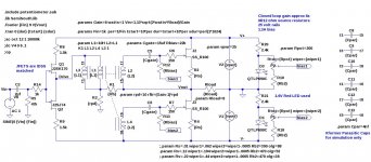
Yes, 10 ohms and 50 ohms giving a nominal closed loop gain of 6x. The actual measured CLG is 5.33x due to losses in the input stage, transformer, and lack of high open-loop gain.neat-o! I presume the feedback resistors are 50ohm and 10ohms like you mentioned before ?
Also are your thd charts are for 2nd and 3rd harmonic only (foo2+foo3) ? - if so presumably the higher orders are very low ?
All significant harmonics are included. The higher harmonics are very low.
hmmm... that gain figure looks oddly low .... it appears that there might be some local feedback going on for your top fet due to return to ground path through the bias network. Or maybe i'm just imagining that 🙂 anyway great stuff mate!
Ilquam,
would using a R divider as Kasey has and as ZM suggested allow for modulation of top fet through bootstrap or other techinques?
would using a R divider as Kasey has and as ZM suggested allow for modulation of top fet through bootstrap or other techinques?
hmmm... that gain figure looks oddly low .... it appears that there might be some local feedback going on for your top fet due to return to ground path through the bias network. Or maybe i'm just imagining that 🙂 anyway great stuff mate!
Here are the equations:
OLG = open-loop gain of the amplifier
X is the input
Y is the output
r1=50 ohms, the feedback resistor from the output
r2=10 ohms, the feedback resistor to ground
G = (r1+r2)/r2 is the nominal gain defined by the feedback network
Z = Y/G is the voltage on the feedback node into the bottom of the transformer primary, (ignoring losses due to current thru the transformer).
Y = OLG*(X-Z) is the equation for a differential amplifier relating its output to the difference of it 2 inputs.
solving the equations we get
CLG = (OLG*G)/((OLG+1)*(G-1)+1)
With OLG=53 (as measured) and r1=50, r2=10 we get
CLG=5.4
Here is my guess at the F6 design, built with Semisouth R100s and the Jensen JT-123-FLPCH transformer.
(best Darth Vader voice)
Impressive
😎

lost in translation
Lhquam, firstly congrats are due for the first build in this thread, your results are inspirational for my efforts. I need a bit of handholding to fill out my understanding so please excuse this rather pedantic post.
Such simple circuits give me a great opportunity to learn more about fet amplifiers and hopefully I get a nice amp as well at the end of the day in addition to some knowledge!
I'm trying to reconcile the gain we're seeing with the fets datasheet and think about reasons they might differ and implications arising (the chief one whether my understanding is in fact correct and therefore the answers will help my improve my comprehension.)
I worked backwards from your observed results as follows from blacks feedback formula (rearranging to solve for OLG);
Standard formula to determine closed loop gain (acl) given known open loop gain (olg) and feedback fraction (b)
acl=aol/(1+b*aol) [using the variables in your post gives same results as yours above]
rearranging to solve for aol gives us:
aol = acl/(1-b*acl).
Now substituting your measured results: acl = 5.33, b=10/60 to derive aol, we get aol = 47.7 or approx 48. This compares to the 53 measured olg which you got. Think were in the same ballpark here so no big issues so far.
Therefore each fet gives us 48/2=24x of gain.
Now lets work out what this implies for the fets transconductance.
Using the equation for common source amplifier with source degeneration, we have stage gain A = - (gm*rl)/(1+gm*rs) .
Rearranging to solve for gm, we get:
gm = A/(rl - A*rs). [this makes intuitive sense also , eg if rs = 0, A=gm*rl which is the usual relationship were familiar with]
Substituting A=24, rl = 8, rs=0.12 we get gm = 24/(8 - 24*0.12), ie gm = 4.7 S approx. Looks reasonable, until....
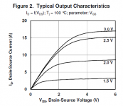
This is the point where I'm flummoxed. Take a look at the datasheet extract below. We don’t see transconductance specified in the datasheet for this part so I used visual inspection of the 100 degrees celcius chart. The 25 degrees gives larger S but seems irrelevant, and 150 degrees gives slightly smaller S but is probably way too hot.
We can see that a 0.5V change in vgs causes Ids to change by 5 to 7 amps depending on vgs. Taking the worst case of 5, this implies transconductance of 5/0.5 = 10S. But the fets transconductance we derived from above observed results (after taking care to correct for source degeneration rs) gives us a measured value of only 4.7 S.
We seem to have 'lost' half of the fets transconductance...
Therefore we need to isolate the reason (combination of ?)
a) R100 fets are performing way below what the datasheet implies.
b) Measurement/logic/math error.
c) Some other feedback is taking place around the output stage.
d) I'm just bonkers.
I'll try to measure (a) tonight and will leave it to anyone who cares to highlight (b) and/or (d). If it happens that (c) is the case, I think we just need to take care that it is same amounts for top and bottom fets.
Again, sorry for the long post...
Lhquam, firstly congrats are due for the first build in this thread, your results are inspirational for my efforts. I need a bit of handholding to fill out my understanding so please excuse this rather pedantic post.
Such simple circuits give me a great opportunity to learn more about fet amplifiers and hopefully I get a nice amp as well at the end of the day in addition to some knowledge!
I'm trying to reconcile the gain we're seeing with the fets datasheet and think about reasons they might differ and implications arising (the chief one whether my understanding is in fact correct and therefore the answers will help my improve my comprehension.)
I worked backwards from your observed results as follows from blacks feedback formula (rearranging to solve for OLG);
Standard formula to determine closed loop gain (acl) given known open loop gain (olg) and feedback fraction (b)
acl=aol/(1+b*aol) [using the variables in your post gives same results as yours above]
rearranging to solve for aol gives us:
aol = acl/(1-b*acl).
Now substituting your measured results: acl = 5.33, b=10/60 to derive aol, we get aol = 47.7 or approx 48. This compares to the 53 measured olg which you got. Think were in the same ballpark here so no big issues so far.
Therefore each fet gives us 48/2=24x of gain.
Now lets work out what this implies for the fets transconductance.
Using the equation for common source amplifier with source degeneration, we have stage gain A = - (gm*rl)/(1+gm*rs) .
Rearranging to solve for gm, we get:
gm = A/(rl - A*rs). [this makes intuitive sense also , eg if rs = 0, A=gm*rl which is the usual relationship were familiar with]
Substituting A=24, rl = 8, rs=0.12 we get gm = 24/(8 - 24*0.12), ie gm = 4.7 S approx. Looks reasonable, until....
This is the point where I'm flummoxed. Take a look at the datasheet extract below. We don’t see transconductance specified in the datasheet for this part so I used visual inspection of the 100 degrees celcius chart. The 25 degrees gives larger S but seems irrelevant, and 150 degrees gives slightly smaller S but is probably way too hot.
We can see that a 0.5V change in vgs causes Ids to change by 5 to 7 amps depending on vgs. Taking the worst case of 5, this implies transconductance of 5/0.5 = 10S. But the fets transconductance we derived from above observed results (after taking care to correct for source degeneration rs) gives us a measured value of only 4.7 S.
We seem to have 'lost' half of the fets transconductance...
Therefore we need to isolate the reason (combination of ?)
a) R100 fets are performing way below what the datasheet implies.
b) Measurement/logic/math error.
c) Some other feedback is taking place around the output stage.
d) I'm just bonkers.
I'll try to measure (a) tonight and will leave it to anyone who cares to highlight (b) and/or (d). If it happens that (c) is the case, I think we just need to take care that it is same amounts for top and bottom fets.
Again, sorry for the long post...
Attachments
I'm not convinced there is voltage gain from the top FET? The input is G-S, the output is the Source. It's Common Drain/Source follower 😉Therefore each fet gives us 48/2=24x of gain.
my vote is for
Would that put your calculation results where you think they should be?b) Measurement/logic/math error...
- Home
- Amplifiers
- Pass Labs
- F6 Amplifier