Something VERY bad is happening there🙁.I didn't have this problems even on test board.Post board layout.
adjustments were made as said by thienchaySomething VERY bad is happening there🙁.I didn't have this problems even on test board.Post board layout.
Attachments
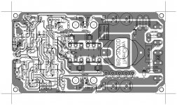
I know this board,i allready commented on it.
Distance between output transistors and buffering capacitors is huge!!,but it should work at 1 or 2 amps.You should remake it for full power.
Distance between output transistors and buffering capacitors is huge!!,but it should work at 1 or 2 amps.You should remake it for full power.
i dint get u.....exactly what u wanna say,,,the capacitors on the supply rails????????I know this board,i allready commented on it.
Distance between output transistors and buffering capacitors is huge!!,but it should work at 1 or 2 amps.You should remake it for full power.
at fulll power means??????????/😱
Yes,those capacitors,they should be very close to output transistors.And ground is very bad,it has loops and and is it long and thin.You can somewhat fix this by using a ground plane on the other side conectata in 10 points butthe capacitors have to be moved.
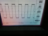
can this be the cause for my problem....even with no loads...i got distorted square wave...if i would have got distorted sine wave i would have said there is ground problem...i used 33uh coil and 0.47uf cap for output filteringYes,those capacitors,they should be very close to output transistors.And ground is very bad,it has loops and and is it long and thin.You can somewhat fix this by using a ground plane on the other side conectata in 10 points butthe capacitors have to be moved.
what does this means????????You can somewhat fix this by using a ground plane on the other side (conectata in 10 points butthe capacitors have to be moved).
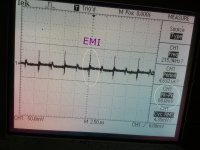
the freq response is before output inductor or after output inductorHi CPX
EMI 4.3mV only no problem for 2CH
see my DSO Picture
Regards
MANOJ
Hi CPX
EMI 4.3mV only no problem for 2CH
see my DSO Picture
Regards
MANOJ
Where is that measured..on the supply or with the probe shorted at a certain distance?
Please post a picture of your amplifier(of both modules)
Please post your syncronizing schematic or explian how you did it.
Thanks.
Last edited:
It means that you can make a new board with ground plane on the other side and you can connect ground to that ground plane in at least 10 points.what does this means????????
Hi CPX
EMI tested input GND on PCB(DSO ground connected to PCB Main GND or supply GND )
Regards
MANOJ
EMI tested input GND on PCB(DSO ground connected to PCB Main GND or supply GND )
It is before coilthe freq response is before output inductor or after output inductor
Regards
MANOJ
i also had the same freq response but it did not turn sine wave after coil....it was still square wave with a distorted formHi CPX
EMI tested input GND on PCB(DSO ground connected to PCB Main GND or supply GND )
It is before coil
Regards
MANOJ
Ok,please post answer to my other questiona when you have time.Thanks alot🙂.Hi CPX
EMI tested input GND on PCB(DSO ground connected to PCB Main GND or supply GND )
Regards
MANOJ
CPX,
can u tell me what can be the reason that output freq is not turned into sinewave after coil...should i increase the inductance and cap...or should i decrease the inductance and increase the capacitor...even if the freq was incorrect the output was so hard and surprising but with noise..
can u tell me what can be the reason that output freq is not turned into sinewave after coil...should i increase the inductance and cap...or should i decrease the inductance and increase the capacitor...even if the freq was incorrect the output was so hard and surprising but with noise..
No..Only if coil has HUGE parasitic capacitance,like 10uf or so.
how to check that
With signal generator and oscilloscope,but if it measures corectly on RLC bridge then is not that.
people are asking for pictures of your pcb, soldering, inductor and you still haven't posted anything. you haven't even replied to what i've said in your thread and in here.from last couple of days i'm trying to ask something but hell with this post nobody is replying....everybdy is busy with there own stuff.....tell me if this place is whole piece of *hit
where's the picture to your pcb huh? any picture to your inductor? did you made any gaps to avoid saturation to it? what type of material huh? where's the signal trace to your mosfet huh?
bitch all you want. nobody is gonna help you if you don't provide anything to help with.
Hi Sweetperfume
greetings have PATIENCE i started this thread i took me a year to get the ucd amp working 30 IR2110 ics smoked out but the experience taught me something check everything carefully components shorts on pcb diodes you use dont PANIC all the designs are working i have tested them all
warm regards
andrew lebon
- Home
- Amplifiers
- Class D
- UCD 25 watts to 1200 watts using 2 mosfets