Diy curve tracer psu. Need 36V+ and about 5A of clean power. I could do big clc, but didnt know if that was adequate as i think the needs for big Class A power amp are not as great in comparison to digital baseed stuff.
basic know how
LM317 PASS TRANSISTOR REGULATOR - Electronic Circuit and Kit - freecircuit.net
And if you have to stay with SJDP only, you just combine the two sketches
I have posted into one attached.
The new negative voltage reference will set both JFets to the selected current bias, pot in the voltage divider will set the output node to the ~half of the supply voltage. Just find the lowest value for R2, that will work for
your speakers and your ears (again, it's a balancing act). Here R4 will be tens KOhm.
So we have come full circle with some nice changes. We have traded self bias for fixed and added feedback to improve Zout. Nice. Is the top biasing mechanism, consisting of V divider and cap, referred to as a gyrator. Ratio of R6/R5 set gain, correct.
<<Is the top biasing mechanism, consisting of V divider and cap, referred to as a gyrator?>>
No. C2, 300 µF is just a coupling capacitor, and, as demonstrated, is not unavoidable. Gyrators, generally, convert impedances - one into another.
The name of this whole arrangement is SRPP.
<<Ratio of R6/R5 set gain, correct?>>
Not exactly. Since the OL gain here (2×Rload / R2) is not high enough to sacrifice for the FB, I suggested to increase it at the expense of some other parameters by reducing R2. So, for the CL volt gain of let's say 15, that ratio may be ~30.
Besides, R5 will be acting together with C1 and Signal source impedance in series. This is why I stressed the requirement for C1 value. And I have to remind you, that to drive that high and nonlinear Cin of power FETs you will need pretty low source Rout with good output current capability.
http://www.diyaudio.com/forums/pass-labs/190438-ss-120r085-depletion-mode-jfet-3.html#post2688498
The last paragraph in this post:
http://www.diyaudio.com/forums/pass-labs/201655-lamp-simple-sit-amp-24.html#post3038629
is a good illustration to what I have said here.
http://www.diyaudio.com/forums/pass-labs/201655-lamp-simple-sit-amp-24.html#post3038629
is a good illustration to what I have said here.
Last edited:
Does this seem to be a reasonable and accurate description of what is going on?
http://valvewizard2.webs.com/SRPP_Blencowe.pdf
It suggest that the when attached to a load, the top fet is in parallel with the load.
http://valvewizard2.webs.com/SRPP_Blencowe.pdf
It suggest that the when attached to a load, the top fet is in parallel with the load.
Last edited:
it always is
just imagine that top one as CCS
then imagine that that CCS can be modulated to our liking
and it is - by AC going through drain resistor of lower one
just imagine that top one as CCS
then imagine that that CCS can be modulated to our liking
and it is - by AC going through drain resistor of lower one
So much pressure toget this right now. I love it. Feelslike i am back in school,but school is fun this time. Thank youboth,very much. I nned to go delete my sudscription to blowtorch thread. Instead of brilliant men advancing audio, universal ******* contest.
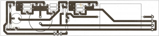
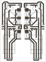
I redid the boards and etched them last night. I have a question about the Rs for the lower fet. Sy is a big fan of LED bias in some of his tube stages. I believe he says that they were tested and found to be quieter than reistors in terms of noise and offer other advantages, such as lower AC impedance. While an LED is not possible at these bias levels, It might be an iteresting experiment. I caould do mulitple, but the number would be too great. This got me thinking about the diodes from the F5. In theory, thewre should be little difference in the two, with the main difference probably being Vf and AC impedance. The diodes from the the F5T, have a larger Vf than I was looking to use, but there are some failry inexpensice schottky diodes with lower numbers. What do you think of the idea and how do i test the AC impedance of one of them.
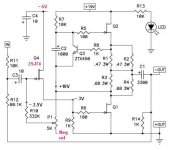
Since folks are curious how to modify the amp camp amp for depl SemiSouthes, I will attach an example (basic idea) where it belongs.
Clearly, the difference is with the front end circuit.
You will need 2SJ74 V, BL.
You will need an additional neg volt supply, probably up to -10V,
and it will be used to feed the neg volt reference, where the lower end of P1 will be connected.
So, I have marked a few test points to give the ballpark values.
For Q2 SemiSouth depl transistor connection, pick the solution
that works for you (discussed in this thread).
Attachments
I will try original circuit, then add FE to see what it may offer in improvement. Not getting much done, as i have matching left that is consuming my time. Doe sthe BJT addition offer improvement because of stable nature of Vbe drop?
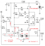
I have not simulated this yet so I don’t know if it will work as drawn. I know this is a depletion Jfet thread but it may be more advantageous to do the Camp Amp like I have drawn it here.
- The SJEP120R100A only costs $28 each vs. $41.08 for the SJDP120R085 at newark.com
- The top MOSFET can also be swapped out without any changes for the JFET making this an all JFET amp.
- There is no need to use P-type Jfets which tend to be harder to find. Moser sells the 2SK170 but not the 2SJ74
- You can replace the two LEDs with an ultra-low noise shunt like ADR530 if preferred (Just watch the current limit).
- I am not sure if the charging of the cap will cause turn on thump?
- The LED’s should be selected to get a drop of about -3.0~-3.5 volts.
Attachments
Last edited:
buzzforb, your graph was at 25C? The threshold will shift down with temp going up. It would be nice to know the threshold at 75C, or something like typical operating temp.
Also, Id up to 2A with Rs bias would be nice. Thx 😀
Also, Id up to 2A with Rs bias would be nice. Thx 😀
Ill put one in the oven and then test. Will be interesting when the kids ask what i am cooking for dinner😀 That graph shows response up to almost 3A. Rs testing will be tougher with current setup. May have to do the old fashion way. I tested this way for two resons, it was easy, and i plan to try without Rs for the fun of it. Got boards almost redrawn and should be able to move through the different iterations. Might be a week or two, as i haev some other matching to finish this week.....hopefullly!
Buzz, your DR085 data looks very suspicious. Gm at ~1A is only (0.3A / 0,1V =) 3S, and drops with current very quickly. And this is @25V Vds? Seems very low.
I am judging only by the d/s fig 4.
Are you sure that 25V stays stable throughout the measurement process? Needs monitoring with an additional voltmeter between D and S.
Are you sure that Vgs steps are coming stable in value (and no excessive gate leakage and high gate drive output resistance to affect this)? Needs monitoring
with an additional voltmeter between G and S.
I was interested in the temp. relative numbers. But, now that you mention it, how did you get these data points?
Actually, I expect something on the order of -4Vgs for Ids of 2A at temp??? 2 ohm Rs w/maybe 15Vds - 25Vds for a self bias test...
Thx 😀
Actually, I expect something on the order of -4Vgs for Ids of 2A at temp??? 2 ohm Rs w/maybe 15Vds - 25Vds for a self bias test...
Thx 😀
Buzz, your DR085 data looks very suspicious. Gm at ~1A is only (0.3A / 0,1V =) 3S, and drops with current very quickly. And this is @25V Vds? Seems very low.
I am judging only by the d/s fig 4.
Are you sure that 25V stays stable throughout the measurement process? Needs monitoring with an additional voltmeter between D and S.
Are you sure that Vgs steps are coming stable in value (and no excessive gate leakage and high gate drive output resistance to affect this)? Needs monitoring
with an additional voltmeter between G and S.
Could be possible, as this is particluar measurement is pushing the curve tracer beyond its preset current limits. Trying to cheat the system. I will test again using standard settings and see what happens. The Yfs did seem low to me. Should have set off alarms.
Last edited:
- Status
- Not open for further replies.
- Home
- Amplifiers
- Pass Labs
- SS 120R085 Depletion Mode Jfet