I would have done six years ago the easiest GCLM3875. Did not use the PCB. Only a few resistors, capacitor structures formed.
Now I miss it and want to improve it so that my friends like it was made very easy.
LM3875, LM4766 I liked them.
Now I miss it and want to improve it so that my friends like it was made very easy.
LM3875, LM4766 I liked them.
Attachments

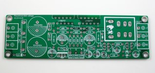
Complete Reference style 47LAB 3875.
Reference 50 watts output power versions. Two 2200UF capacitor.
Integration by adding the protection circuit board .10 * 2 relay reliable.
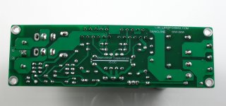
Backside of the PCB, DC location, said the short here, the negative feedback using DC.
Reference 50 watts output power versions. Two 2200UF capacitor.
Integration by adding the protection circuit board .10 * 2 relay reliable.
Backside of the PCB, DC location, said the short here, the negative feedback using DC.
I like the sound of the IC. My opinion, than the LM4780, LM3886 more flavor.
For this reason it's slower than the LM3886, there will be a very good flavor.
For this reason it's slower than the LM3886, there will be a very good flavor.
LJM - what exactly did you design?? It's just a data sheet implementation.
You're kidding, right?
Curious to see where this goes, not sure what flavour an amp is supposed to have, strawberry? vanilla?.......
Or single Malt ? Like now.....Nadurra ! 
It's late, I'm off to bed !
Edit: Pretty big relay on that tiny board. Looks interesting.Will do a closer inspection tomorrow !
Looks like a text book implementation with relay protection. Neat . What brand is that relay ?
PCB's available ?
It's late, I'm off to bed !
Edit: Pretty big relay on that tiny board. Looks interesting.Will do a closer inspection tomorrow !
Looks like a text book implementation with relay protection. Neat . What brand is that relay ?
PCB's available ?
Last edited:
Nice PCB. 2200uF is a bit low for my liking. I prefer the protection and PSU seperate but that just my preference.
Interesting. I used a relay of this sort in one of my amplifiers and it has since failed, or at least became unreliable. Not because it has ever tripped, but I presume just from contamination of the contacts by the air, so I presume a fully sealed type is a better option.
Probably going to be trying out a solid state MOSFET system to replace it, looking like this may be the way to go for DC protection really.
Probably going to be trying out a solid state MOSFET system to replace it, looking like this may be the way to go for DC protection really.
Or single Malt ? Like now.....Nadurra !
It's late, I'm off to bed !
Edit: Pretty big relay on that tiny board. Looks interesting.Will do a closer inspection tomorrow !
Looks like a text book implementation with relay protection. Neat . What brand is that relay ?
PCB's available ?
132MM * 40 MM
Its small size.
Interesting. I used a relay of this sort in one of my amplifiers and it has since failed, or at least became unreliable. Not because it has ever tripped, but I presume just from contamination of the contacts by the air, so I presume a fully sealed type is a better option.
Probably going to be trying out a solid state MOSFET system to replace it, looking like this may be the way to go for DC protection really.
I am not worried that this relay has a large contact area.
Silver alloy has a very high life. I have more than five years without failure in the other circuit protection board.
It has a current capacity .10 A * 2
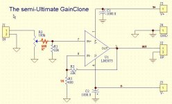
Have you used a 100k volume potentiometer with the Rin=22k68 as shown in the schematics?
Is it a linear track potentiometer with a log law faking resistor?
Is it a linear track potentiometer with a log law faking resistor?
Have you used a 100k volume potentiometer with the Rin=22k68 as shown in the schematics?
Is it a linear track potentiometer with a log law faking resistor?
I will use the 20K volume. Excessive volume, resistance will bring more noise.
When the impedance to reduce noise will be reduced.
10k pot feeding Rin=22k should be better.
A lower value pot will reduce the variation in output offset as you turn the volume up/down.
A lower value pot will reduce the variation in output offset as you turn the volume up/down.
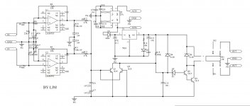
I love a lot of things about your PCB layout. But one thing that I think could be better is the placement, relative to the chips' power pins, of the decoupling/bypass capacitors, and, to some extent, the main caps.
The small-value decoupling/bypass caps need to be right AT the power pins. If they are more than a millimeter or two from each pin, they do no good for high-frequency stability problems.
It would also help to have at least another 220 uF or more of decoupling cap for each power pin, but right AT the pins, if possible (or at least with less than one inch of total trace and lead length).
And if there is any way to get the main caps closer to the chips' power pins, and symmetrical with respect to the distances to the two channels' power pins, then it would be almost perfect.
I love a lot of things about your PCB layout. But one thing that I think could be better is the placement, relative to the chips' power pins, of the decoupling/bypass capacitors, and, to some extent, the main caps.
The small-value decoupling/bypass caps need to be right AT the power pins. If they are more than a millimeter or two from each pin, they do no good for high-frequency stability problems.
It would also help to have at least another 220 uF or more of decoupling cap for each power pin, but right AT the pins, if possible (or at least with less than one inch of total trace and lead length).
And if there is any way to get the main caps closer to the chips' power pins, and symmetrical with respect to the distances to the two channels' power pins, then it would be almost perfect.
I have the same idea repeatedly to change the location of the power supply and IC.
0.1UF capacitor. I think it is close to the IC is perfect.
In practical applications, the LM3875 low power requirements. This capacitance is almost not affected from the point of view the actual performance.
It can work very well, to increase the power of the copper area to reduce the impact of power.
Yes. If the copper area is large then maybe it could act almost like power and ground planes and might make the very close cap placement less important.
The inductance was all that I was really thinking about, for that. A worst-case (best-case?) transient 3886 slew-rate from 0 to rail would need at least 200 uF decoupling per rail with less than 20 or 30 nH in each of their connections to power pins and gnd, but only IF you arbitrarily decided that the rail voltage should not be disturbed by more than 0.1 Volt or so, by such a transient. So maybe it's OK, since even a much larger rail disturbance might not matter too much, with these chips.
The high-frequency bypassing, I'm not so sure about. But it might be best to add some caps on the bottom of the board, or maybe soldered directly to chip's pins, or maybe surface-mounted somewhere from pin pads to gnd (Sorry I didn't have time to look at the layout again, right now.). Sometimes it might not oscillate all the way and might not be obvious-enough, but maybe could still affect the sound. No way to really know without a good scope and some fast-rising pulse edges to bang into it (or some RF in the air). Without effective bypassing, there might be a "hidden" positive feedback path from power rails to input, internally, for high frequencies.
I forgot to look to see if you put any low-pass RF filter for input. I would at least place the pads for it to be optional.
Again, that's an extremely-good layout. Good work.
Last edited:

Gootee
No I'm not kidding. The supplementary circuitry may have been designed by him but the amp circuit itself is standard so what bit of that did he design? It's just like all the zillions of other gainclones out there. In fact, it looks exactly the same as the Peter Daniel Audiosector implementation.
No I'm not kidding. The supplementary circuitry may have been designed by him but the amp circuit itself is standard so what bit of that did he design? It's just like all the zillions of other gainclones out there. In fact, it looks exactly the same as the Peter Daniel Audiosector implementation.
Last edited:
- Home
- Amplifiers
- Chip Amps
- I designed the GC LM3875