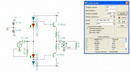
OK, I found a regular diode with the proper forward voltage drop, and I used them in this circuit. Even if I lowered Re to 0.5 ohms, there was still several hundred mV across it with over 0.5A flowing through the transistors. Distortion was low, but replacing the regular diodes with the LED's made the distortion even lower. I raised the Re values also when I installed the LED's. Quiescent current is something like 50mA in this circuit.
Thanks again for your suggestions.
@ 20vp-p input, 20kHz, distortion was still only 0.02% into 600 ohms (over 14Vrms output).
Thanks again for your suggestions.
@ 20vp-p input, 20kHz, distortion was still only 0.02% into 600 ohms (over 14Vrms output).
Attachments
Last edited:
Then adjust the CCS current downwards until the output bias current reaches what you prefer.
You can ask the simulator what the Vbe of each output device is @ your chosen current.
You can ask what the voltage cross Re is at your chosen current.
You can ask what the diode Vf is at your chosen current.
Then use a bit of guessing to select a new value for the CCS current.
You can ask the simulator what the Vbe of each output device is @ your chosen current.
You can ask what the voltage cross Re is at your chosen current.
You can ask what the diode Vf is at your chosen current.
Then use a bit of guessing to select a new value for the CCS current.
Could you adjust the output Re values to ensure that you have optimum ClassAB bias voltage and ClassA output current up to your desired limit?
Um.... IIRC, this is a preamp, not a power amp. If so, there's no need to worry about it transitioning to class B. It's probably more linear in pure class A with the higher voltage across the emitter resistors, as it was.BTW, I am not expecting the ClassA performance to improve.
It's the transition to ClassAB that I am trying to help you with.
He has chosen 40mA of output bias. That limits the ClassA output current to <80mApk. What if the demand ever equals or exceeds 80mApk?
The amp is capable of delivering a lot more than 80mApk.
Why should we/he not design for that transition to be as good as possible, just in case it ever happens (headphones?).
The amp is capable of delivering a lot more than 80mApk.
Why should we/he not design for that transition to be as good as possible, just in case it ever happens (headphones?).
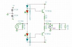
This version is capable of driving the 50ohm load with 20nF capacitance with 0.03% distortion @ 10Vp-p input, 20kHz. Output voltage is 6.68Vrms. Bandwidth is good with a smooth roll off above 1MHz. Quiescent current in each transistor is 110mA.
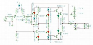
There's something different about these TIP29/TIP30 transistors because I tried the standard single diode per transistor biasing arrangement and they were virtually turned off. Distortion was really bad, even with 0.1ohm Re. I tried 2 diodes per transistor and things improved. I removed the diodes and replaced them with the LED and it worked even better. Voltage drop across each LED is 1.47V.
I dunno, this should work with just the single diode (750mV forward voltage).
Anyway, I guess you'd call this current version "deep class A".... 😱 about 2.6 watts dissipation just sitting there... well, maybe not, but this is all new to me..
I suppose this could be a stand alone buffer for a preamp or something. "Why's your preamp so warm?".... "Class A baby!" <g>
Attachments
Last edited:
If you adopt two single diodes then ask sim what is the voltage across each diode.
Now ask the sim what is the voltage across each output transistor (Vbe).
ask the sim what is the voltage across the Re.
Add and subtract all these voltages and the answer (pencil & paper) should come to exactly ZERO. If not, then you are not understanding what the sim is predicting for you.
Vf diode1 + Vf diode2 - Vbe transistor1 -Vbe transistor2 - Vre resistor1 -Vre resistor 2 = zero !
That is the complete string of components in the loop around the output stage.
Sorry I've been busy with other things on other threads. I got some inspiration and now I've got a small power amp! It makes 15 watts at clipping (which is the 0.5% distortion point) into 8 ohms/1nF @ 1kHz. It takes about 2.7volts p-p to get there though.... Distortion is far lower at say 12 watts (0.002%). Bandwidth is good.
If the load is 32 ohms, like a pair of headphones, and the feedback is increased to reduce gain to 6dB, distortion at a little over 1 volt output (where most headphones are producing over 100dB), distortion is tiny. (0.000100%)
Thanks again to everyone for your kind help. Much appreciated! I want to build this now.
Attachments
Last edited:
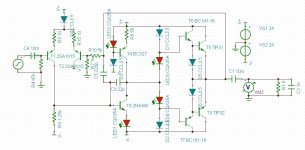
I found a mistake in my previous schematic. The CRD's in the follower loads for T6 and T7 didn't have enough voltage across them to function as CCS's. So, I substituted ordinary diodes and it works fine. Distortion is 7.6x10^-5% @ 1kHz, 1.12Vrms output into 32ohms, which is maximum loudness for most headphones.
Attachments
The diodes D5, D6 in the T3, T5 bases will just induce even-order distortions at high level signals. at low levels they are just uselles.
I don't know what did you simulate, but they will start to "open" in the same voltage range that transistors work.
I don't know what did you simulate, but they will start to "open" in the same voltage range that transistors work.
The diodes D5, D6 in the T3, T5 bases will just induce even-order distortions at high level signals. at low levels they are just uselles.
I don't know what did you simulate, but they will start to "open" in the same voltage range that transistors work.
Thanks for your input. I'm not sure I understand your comments. What is your suggestion about what to do with the diodes then?
As I said, distortion was measured at maximum typical output of 1.12Vrms into 32 ohms, which would be about right for headphones.
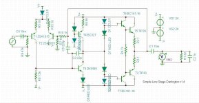
As I see it, I just did a variation on this circuit. If there's something seriously wrong with what I did, I'd like to know about it, obviously. It's from a basic circuits web site here:
Push-Pull Output Stage
I just replaced the two resistors with transistors. Or, another way to look at it, which is I think the way I came about this, was to modify a Darlington pair by adding the diodes. It seems to work, though I don't claim to understand it completely.
Push-Pull Output Stage
I just replaced the two resistors with transistors. Or, another way to look at it, which is I think the way I came about this, was to modify a Darlington pair by adding the diodes. It seems to work, though I don't claim to understand it completely.
Attachments
Put back the emitter resistors.
Adjust the output bias current by adjusting the diode current.
Why?
because it's what you had in post225 and preceding.
Adopting the darlington confused the issue. You need emitter resistors even when it is a darlington.
Adopting the darlington confused the issue. You need emitter resistors even when it is a darlington.
because it's what you had in post225 and preceding.
Adopting the darlington confused the issue. You need emitter resistors even when it is a darlington.
I have analyzed each of the two output arrangements. Given the same operating point for the output transistors, the same load, the same source and the same supply voltage, the more complex one has a little bit less distortion than the more simple one. It's about 50% less with the more complex one, in this case, 0.42% vs 0.27% (driving an 8 ohm/1nF load with 5V input). The TIP29/30 really like a lot of current.
Another way to look at it is the clipping level for each one, which I randomly define as the 0.5% distortion level. The more complex circuit will put out almost 12Vrms at that point (18watts), vs. a little bit less than 7Vrms (6.1watts) for the more simple one.
Of course, these differences only really show up when driving a low load.
Of course, these differences only really show up when driving a low load.
Unlike that example, you've connected the midpoint of the diodes to the amplifier's output, which won't help anything. The purpose of the diodes in that circuit is to set the bias voltage between the bases of the output transistors. In your circuit that function is fulfilled by the LEDs.It's from a basic circuits web site here:
Push-Pull Output Stage
What would be useful in your circuit is a resistor (say 100 ohms) between the bases of T3 and T5, to ensure there is always significant current flowing in T6 and T7.
I agree with Andrew that you should use emitter resistors too, to set/limit the output stage idling current. If the voltage across your LEDs is slightly higher than you expect, then the current through the output stage will be much higher than you expect.
IIRC, your simulator is telling you there's about 1.47V across each LED. That seems much too low. Normal is about 1.7V. Maybe you could measure the voltage drop across the actual LEDs you plan to use, and compare that to the sim's opinion? Aren't there other, more realistic LEDs in your simulator's library?
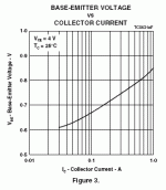
The pic below is from the Bourns TIP29 datasheet. It gives an idea what happens if you increase Vbe from say 700mV to 900mV. What it doesn't show is that the current also increases with temperature. So more current causes more heat which causes even more current etc until the transistor blows. That's called thermal runaway.
Attachments
Unlike that example, you've connected the midpoint of the diodes to the amplifier's output, which won't help anything. The purpose of the diodes in that circuit is to set the bias voltage between the bases of the output transistors. In your circuit that function is fulfilled by the LEDs.
What would be useful in your circuit is a resistor (say 100 ohms) between the bases of T3 and T5, to ensure there is always significant current flowing in T6 and T7.
I agree with Andrew that you should use emitter resistors too, to set/limit the output stage idling current. If the voltage across your LEDs is slightly higher than you expect, then the current through the output stage will be much higher than you expect.
IIRC, your simulator is telling you there's about 1.47V across each LED. That seems much too low. Normal is about 1.7V. Maybe you could measure the voltage drop across the actual LEDs you plan to use, and compare that to the sim's opinion? Aren't there other, more realistic LEDs in your simulator's library?
The pic below is from the Bourns TIP29 datasheet. It gives an idea what happens if you increase Vbe from say 700mV to 900mV. What it doesn't show is that the current also increases with temperature. So more current causes more heat which causes even more current etc until the transistor blows. That's called thermal runaway.
Thanks! When I was working on it yesterday, I disconnected the diodes in the emitter circuit from the output since it made distortion worse.
I'll take a look at the LED situation. It was 1.47V for 3.5mA. I think the voltage goes up with more current.
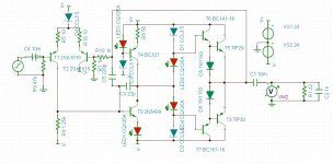
The attached version has 0.0001% distortion driving 32 ohms @ 1.4Vrms, which like a headphone load.
I'll try your suggestions when I have the time. Thanks again.
EDIT: ok, I forgot I had the Bob Cordell spice model for the red LED. I replaced all of them in the circuit with Bob's. Now I have to rebalance the LTP and adjust other values.
Attachments
Last edited:
Now that the schematic is just about correct, start investigating what voltages exist around the circuit.
Start investigating what currents are flowing around the circuit.
Start understanding why the circuit works.
Remember I was trying to get you to investigate the voltages around the output stage loop.
Do that now for this latest schematic.
You will find an anomaly. The red LED voltages needs to be VERY low to get your circuit to bias properly.
- Status
- Not open for further replies.
- Home
- Source & Line
- Analog Line Level
- discrete op amp