i also remember having read multiple times that it is desirable to match parallel output devices in the output stage of amps but i m not sure why...could you (or someone else) care to explain? i understand that heat load will be shared even but that is it...
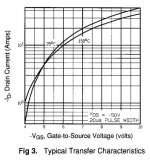
also, i understand that having the lowest possible bias through the bjt (see pic) gives lower output impedance, so i m wondering what obstacles do you encounter when lowering to much the bias. is there a sweet spot? in the pic it is around 4mA depending on the mosfet.
To avoid current hogging that leads to a catastrophic sequence.
The output impedance will be a function of the error amp's open loop gain and the current follower's transcoductance. R6 gets to be a CCS and the follower's bias gets to be spared higher to trigger more Gfs if we are after decreasing Zo.
To avoid current hogging that leads to a catastrophic sequence.
you mean that we dont want to be in the bottom portion of the graph in the attachment, where linearity is not so good?
The output impedance will be a function of the error amp's open loop gain and the current follower's transcoductance. R6 gets to be a CCS and the follower's bias gets to be spared higher to trigger more Gfs if we are after decreasing Zo.
yes i just remembered that a jfet had replaced the resistor in the later versions.how about 2 jfets cascoded to further improve Zo?would you advise against it or should i let myself go?
P.S.: just tell me if i get annoying with my questions and i ll get back to my books 🙂
Attachments
We don't want one in a group to draw more current than the others, as it gets hotter it draws even more, vicious circle until it fails and kills some more. So we match them and/or we give them little source resistors like in amps.
To make a cascode is not recommended when you will only have 3.3V and in there you will have to fit one vbe and two Vgs drops. Use a BF245A, its enough low pinch off and low capacitance Jfet good for VHF/UHF amps even.
To make a cascode is not recommended when you will only have 3.3V and in there you will have to fit one vbe and two Vgs drops. Use a BF245A, its enough low pinch off and low capacitance Jfet good for VHF/UHF amps even.
yes indeed, fitting a cascode within around 2.5V 2sj313 Vgs looks pretty lame. forgot about that 🙂.
thanks for showing me bf245a looks better than 2sk170. looks also like it would require very low current to be effective. maybe something like the less available 2sk369 would be a better fit(although capacitance is higher...)?
thanks for showing me bf245a looks better than 2sk170. looks also like it would require very low current to be effective. maybe something like the less available 2sk369 would be a better fit(although capacitance is higher...)?
Attachments
Last edited:
after giving some thought, bf245a might be very nice as current sources in this reg indeed.now i ll try to find a more common shunt mosfet.
thanks a lot salas. now i know better what direction to go to.🙂
thanks a lot salas. now i know better what direction to go to.🙂
Whatever sum of parts you choose see they will have adequate phase margin for stability as a circuit. Good luck.
guys the output mosfet is hot when testing without load and colder with load?
is that correct?
is that correct?
Whatever sum of parts you choose see they will have adequate phase margin for stability as a circuit. Good luck.
ok. i might just not venture into paralleling shunt devices yet.
what do you think about those?
fqp4n20l
http://media.digikey.com/pdf/Data%20Sheets/Fairchild%20PDFs/FQP4N20L.pdf
zvn0124a
http://www.diodes.com/datasheets/ZVN0124A.pdf
IRLU024Z
http://www.irf.com/product-info/datasheets/data/irlr024zpbf.pdf
For 1,2V "disco" (about 150mA):
would it be possible (and benificial) to substitute the v1 "CCS-section" with bc560; - to v1.1 bib with 3 green led? (Then you actually could tweak the bib-board, by mainly substituting the MJE15031 for d45h8 (+ jumper bib-R4, and bib-R6 = 10ohm)
would it be possible (and benificial) to substitute the v1 "CCS-section" with bc560; - to v1.1 bib with 3 green led? (Then you actually could tweak the bib-board, by mainly substituting the MJE15031 for d45h8 (+ jumper bib-R4, and bib-R6 = 10ohm)
ok. i might just not venture into paralleling shunt devices yet.
what do you think about those?
fqp4n20l
http://media.digikey.com/pdf/Data%20Sheets/Fairchild%20PDFs/FQP4N20L.pdf
zvn0124a
http://www.diodes.com/datasheets/ZVN0124A.pdf
IRLU024Z
http://www.irf.com/product-info/datasheets/data/irlr024zpbf.pdf
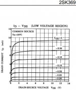
Look how the capacitances enlarge the lower the Vds. Best is the 3rd one for low output voltages for instance. The middle depletion one is out of the question in any case with 0.1S gfs and no sinking ability.
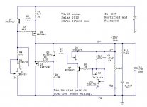
Is it possible to get -3.5V out without modifying the second picture in post 3200?
no. because of the mosfet Vgs. maybe you could get -4V or so. But if you choose a lower Vgs mosfet, maybe you could, just like i m trying to do with the V1.1. i dont know anyone who has tried yet. (the reg you are talking about is attached)
Attachments
Look how the capacitances enlarge the lower the Vds. Best is the 3rd one for low output voltages for instance. The middle depletion one is out of the question in any case with 0.1S gfs and no sinking ability.
yes the third one could be nice at high current, albeit being t0-251.
the little depletion one is rated 160 mA max continuous Id. But looking at the curves, i thought that a characteristic 0.4S and around 5pF Crss at 3.3V could be interesting to test, if only to know what benefit low capacitance can bring. Or maybe this is a bad idea altogether...? Moreover, a shunt device battle Bc560c vs little mosfet could be cool 🙂
for comparison, irf610 has around 50pF Crss at 5V and 0.4S at around 150mA and a better 0.8S at 500mA.
Last edited:
It eats up >6Vin that is the thing.
Quick test with DC in before rectifier diodes:
bib v1.1 has Vin = Vout + 4,3V
disco has Vin = Vout +4,0V
before Vout starts dropping.
So they burn approx the same on input ?!?
Gets more to be mains drop odds away. The disco can be made some less if you don't have enough Tx VAC installed. Let me know to see in to it.
check the voltage drop across the CCS resistor.
That suffers first when mains voltage drops.
If the CCS starts to lose Vdrop then it is no longer a CCS and the attributes of the CCS are lost.
The Shunt part attempts to compensate for the lost CCS current flow by reducing it's own bypass current in trying to maintain output voltage. The reduced current shunt is now not operating at optimum.
Checking output voltage vs input voltage is not the correct way to determine if the CCS + Shunt has sufficient supply voltage.
Check the CCS resistor voltage. It should be substantially constant over the full range of mains supply voltage.
Excuse me for this annoying and maybe repeated question, but can the transistors from the original schematics (like 2SCK170 or IRFP9240) be substituted with others - how critical is it? I plan using these shuns for the 3.3 and 5V rails for my DAC.
- Status
- Not open for further replies.
- Home
- Amplifiers
- Power Supplies
- The simplistic Salas low voltage shunt regulator