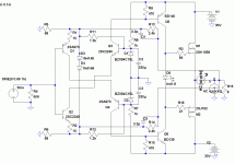
I made a simulation of it: http://i.imgur.com/Aj40T.png
Without the opamp it has a nasty dc offset that cause one side to pull 100mA bias while the other is just at 30-40mA.
With the opamp the output dc offset is in the nanovolts, in the sim i have the bias set to around 70-80mA.
If theres interest in my simulation, i might try and build it.
Without the opamp it has a nasty dc offset that cause one side to pull 100mA bias while the other is just at 30-40mA.
With the opamp the output dc offset is in the nanovolts, in the sim i have the bias set to around 70-80mA.
If theres interest in my simulation, i might try and build it.
I made a simulation of it: http://i.imgur.com/Aj40T.png
Without the opamp it has a nasty dc offset that cause one side to pull 100mA bias while the other is just at 30-40mA.
With the opamp the output dc offset is in the nanovolts, in the sim i have the bias set to around 70-80mA.
If theres interest in my simulation, i might try and build it.
Good luck. Me I am preparing to try one by this simulation attached, hopping for 28.5dB gain at least, and more 2nd order with only 15-18dB feedback (THD sim on edge to clip). Making it on veroboard little by little, have to thread a piece of sink etc. One thing that puzzles me is I saw TO-220 diodes without sinking proposed on the 40W Sziklai board early examples. How can this be when it can draw ~3A peaks per rail on 8 Ohm load at sine wave apex just before clipping... I will see to bolt mine down on the main sink since I will use them for both channels anyway. I know it can be very stubborn to bias up correctly, but I cross fingers I am near by calculations. Will vary/add some basic bias resistors before final installation if necessary.
Attachments
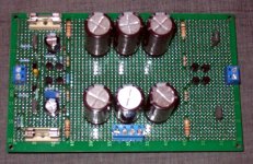
Very neat layout Salas! Shows you a PCB is not really necessary to make a good looking layout.
Those through plated protoboards look neat but are a absolute PITA if you need to replace/move a component.🙁
Takes patience...
Congrats Salas,
Simply, better . . . as they say, the beauty is in its simplicity ... 🙂
Those through plated protoboards look neat but are a absolute PITA if you need to replace/move a component.🙁
Indeed. No allowance for many errors to fix easily. The right hand part channel is mirrored negative. But I won't populate crucial resistors there before I will run the left channel successfully and trimmed for currents. Then I will copy.
Smart move. Just as i build just one channel of my designs for testing and debugging first, and when it works, i tackle the other channel.
SSA Basic
Hi Tekko
I'm so happy that you are the first one to simulate and actually built the sch from my first post. Congratuuulaaations
I don't know if you tried to change R5&R6 from your sch with trimmers and than you can set both BIAS and zero DC at the output. If you will glue together the input BJT pair (thermal joint) the offset will be around +/-10mV when working temperature will be reached.
Please try to play with some parts it will be generously rewarded to you at the end. Have fun. 😉
I made a simulation of it: http://i.imgur.com/Aj40T.png
Without the opamp it has a nasty dc offset that cause one side to pull 100mA bias while the other is just at 30-40mA.
With the opamp the output dc offset is in the nanovolts, in the sim i have the bias set to around 70-80mA.
If theres interest in my simulation, i might try and build it.
Hi Tekko
I'm so happy that you are the first one to simulate and actually built the sch from my first post. Congratuuulaaations
I don't know if you tried to change R5&R6 from your sch with trimmers and than you can set both BIAS and zero DC at the output. If you will glue together the input BJT pair (thermal joint) the offset will be around +/-10mV when working temperature will be reached.
Please try to play with some parts it will be generously rewarded to you at the end. Have fun. 😉
Good luck. Me I am preparing to try one by this simulation attached, hopping for 28.5dB gain at least, and more 2nd order with only 15-18dB feedback (THD sim on edge to clip). Making it on veroboard little by little, have to thread a piece of sink etc. One thing that puzzles me is I saw TO-220 diodes without sinking proposed on the 40W Sziklai board early examples. How can this be when it can draw ~3A peaks per rail on 8 Ohm load at sine wave apex just before clipping... I will see to bolt mine down on the main sink since I will use them for both channels anyway. I know it can be very stubborn to bias up correctly, but I cross fingers I am near by calculations. Will vary/add some basic bias resistors before final installation if necessary.
Hi Salas
It is nice to see you involved in a SSA project. I'm sure you'll make it all right and have a lot of pleasure with the sound of music coming out from your speakers.
Regards Andrej 😉
If it will go well I will see what it has to gain from adding the +/-5V loss due to laterals, maybe regulated with symmetric shunts up to the drivers. Because its so sensitive like a measuring bridge, I am afraid that dynamics can modulate it when hitting full power.
Hehe yes it is sensitive because it is actually a bridge. But except DC sensitivity to be modulated by thermal conditions there is no tendency to be AC modulated or oscilated by max power or at clipping. All my versions tested were stable as a rock.
Esperado also upgraded legendary Elektor's Cresscendo to SSA and he reached bandwidth just bellow 10 MHz, some 1000V/us of slew and he didn't reported any problems. He even claimed that there was actually sound improvement noticed, so all in all very promising informations.
Esperado also upgraded legendary Elektor's Cresscendo to SSA and he reached bandwidth just bellow 10 MHz, some 1000V/us of slew and he didn't reported any problems. He even claimed that there was actually sound improvement noticed, so all in all very promising informations.
No, as long as +/-15V is not affected by harsh PSU conditions. From +/-15V there is quite some current sourced/sinked to the bridge that's why 1000uF are there. But I am sure the main PSU will have enough energy reserve to handle peak and max average consumption. So proper amp power design considerations must be calculated and realized in practice.
I havent actually built it yet, i just simmed it outta curiosity, and if i heat up the soldering iron i'd prolly prioritize my own jfet input bjt or mosfet output designs before going onto this one.
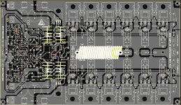
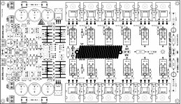
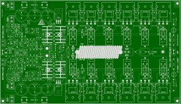
SSA Low Impedance HP 1.2
Hi guys 🙂
Finally, I am proud to announce that the SSA Low Impedance HP design project is prepared. It was a DIY community mutual project since there are ideas, knowledge, effort and of course time & energy of many involved, to offer free SSA amplifier project to all interested. 😉
Happy DIY, enjoy, regards Andrej
P.S. Special thanks to Alex, you're the Man.
Attachments
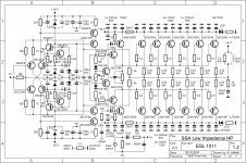
The Beautyest Beast
@ And a special thanks to You Andrej, providing - engineering & sharing the beautiest Power Amp design here on a DiyAudio community @
Happy DIY, enjoy, regards Andrej
P.S. Special thanks to Alex, you're the Man.
@ And a special thanks to You Andrej, providing - engineering & sharing the beautiest Power Amp design here on a DiyAudio community @ - Status
- Not open for further replies.
- Home
- Amplifiers
- Solid State
- Simple Symetrical Amplifier