peranders said:The reason is simple: the amp will oscillate! If you have at least three different stages, input stage, voltage amplification stage, output stage. The bandwidths of all these stages must be carefully matched if you are going to apply feedback.
No...on all counts.
MikeB said:.......what makes a fast transistor a fast one?.......
...Unity gain transition frequency, ft.
mikeks said:
...Unity gain transition frequency, ft.
Hmm, but what is all that about "storagetime" "risetime" "falltime"
"basecapacitance" "outputcapacitance" ?
Shouldn't these parameters really describe the SPEED of a BJT ?
I can't imagine that ft really changes groupdelay for example...
Mike
MikeB said:
I can't imagine that ft really changes groupdelay for example...
Mike
Alas, 'group delay' has little to do with 'delay' per se....
Reply
I have seen several MEYERSOUND amps with Slewrate of 300V/uS and that too without output inductor filter and they are stable all along with 15 meters of speaker wires connections.
Regards,
Kanwar
Hi JOHN,john curl said:Folks, I don't know if I can make better sense of everything that you are talking about, but slew rate is a LIMITING CONDITION that you don't want to approach. Do you need 500V/us? Couldn't hurt! Can you get away with 10V/us? Maybe with a bass amp, even a midrange amp, but not a full range amp, for best solid state audio fidelity.
Now, do some output devices limit slew rate? Yes
Do some input topologies limit slew rate? Yes
Today, with improved devices, the output stage should not limit the slew rate to any significant degree. However, 30 years ago, this was not the case.
However, the most significant limitation to slew rate is both the amplifier gain bandwidth, and the transconductance of the input stage. It can be shown that transistors have so much transconductance, that compensating for this lowers the slew rate below what is acceptable, in most cases.
When you try to make a fast amp, you usually also make it more sensitive to capacitance on the output. This can make an amp oscillate. Protecting an amp from output capacitance with an output coil can compromise the overall sonic quality of a power amp. This is why I choose to designing about 100V/us into my typical designs, today, even though I have designed faster amps in the past. I can remove the output coil, and still remain stable.
I hope that this helps.
I have seen several MEYERSOUND amps with Slewrate of 300V/uS and that too without output inductor filter and they are stable all along with 15 meters of speaker wires connections.
Regards,
Kanwar
Thank you....
Actually, you can adjust 'small-signal' bandwidth by means other than the comp. cap., eg degeneration in input stage, resistor across comp. cap (bad idea!), additional comp. eg input lag comp....etc....while affecting slew rate not one jot....
Hello
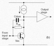
Why a resistor across cdom cap are bad ?
Thank
Bye
Gaetan
Attachments
Last edited:
Gaetan, I can think of several reasons, but my amplifier fu is not strong enough to say which are the biggest problems. My guess would be the main issue is the asymmetry between charge and discharge rates created by putting a bleeder on the cap.
This is an old thread, but an interesting one; came across it as the topic's been much on my mind of late. I'm working on proto board for some low power amplifiers which happens to include a LME49713+LME49600 output and an LME49990+LME49600 output. To my subjective surprise, I hear a difference between 49713 and 49990 with the 49713 being slightly preferable. The parts are better than my measurement gear and so far the things I've tried to tease out differences just give me the measurement limitations back. So I'm trying a theoretical approach instead. 😛 Both output blocks are differential input with 0.1% 1.5k feedback resistors and identical layout and bypassing within the usual 20% XR7 tolerance---medium pitch SOIC and 0805/1206 stuff that should be decently laid out---and both should performance limit on the op amps and not the 49600. The 1.5k feedback network should result in both channels having 110MHz GBP, matched within National's process tolerances, so the primary difference between the channels is the slew rate. That's 22V/us typ for the 49990 and around 100V/us for the 49713 at the tens to low hundreds of mV I'm listening at.
As various folks have observed over the years (off the top my head, the earliest remarks on this are from Walt Jung in 1979) the 20kHz slew rate calculations used earlier in this thread neglect percussion's tendency to be a good approximation of a delta function. I've poked around a bit in the CDs I'm using (the usual 44.1kHz 16 bit) and the maximum slew between adjacent samples in a signal whose voltage envelope varies from +Vpeak to -Vpeak is about 1.3Vpeak. With my roughly 250mV listening envelope that works out to be about 15mV/us for a straight line between the samples. The DAC needs some time to corner on the impusles so the actual slope's somewhat steeper---call it 50mV/us. Or 100mV/us. Or even 1V/us. It's still waaayyy slower than the 49990's 22V/us or the 49713's 100V/us. So, going by the 10x rule of thumb Bob and John and Nelson mentioned earlier in the thread, the 49990 has plenty of slew rate and there shouldn't be an audible difference between it and the 49713.
But I hear a difference. And I'm scoring 100% discrimination in my attempts to approximate blind A/B between the two op amps. Anyone have thoughts on why this might be? (I do have a couple hypothesis, but don't want to bias the discussion to specific ideas.)
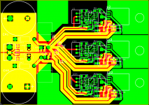
This sounds very interesting - care to post up schematics/diagrams of where these parts are going in the signal chain and how the layout's arranged?
Years ago (before digital) I built a slew rate meter. This was part of an amp (the original Spectral CPU 100) that had a 500V/uS slew rate. The meter was to show off the abilities of the amp. Simple to build (then). I used an analog delay line and measured the voltage differential across the line. Unfortunately with a 500V/uS scale it never moved on music. In fact is was useless until I scaled it to more like 500 mV/uS for music or even record mistracking. Real audio doesn't have much slew BUT the amps with higher slew rate sound better.
This connects to a common problem here. Simply put it is the assumption that if I improve factor "A" (e.g. slew rate) and it sounds better then factor "A" (slew rate) is important. We can only say that the changes that improved factor "A" made it sound better, not that factor "A" is significant.
Separately- slew rate is supposed to be measured as the rate of change of a sine wave generating something like 3% HD, indicating that the feedback is losing control of the amplifier. Possibly for audio that percentage should be more like .1%. Measuring slew rate as how fast the output changes under saturation is really useless. Watch datasheets for this since you will see much higher numbers.
Oh, I'm well aware correlation doesn't imply causation. Schematic and layout attached---J1/J11/J21 are the ins from the active crossover and J2/J12/J22 go to the drivers. Some of the supply bits---100uF and 10000uF caps, diodes, and the regulators---aren't stuffed yet; rails are currently +/-12V off an HP E3620 lab supply with minimal length jumpers tacked to the board to provide continuity. C1/C11/C21 are X2Y caps---they're just a cheaper way of getting a well matched pair of C0G 100pFs. Board's 3 by 4.25 inches.
Attachments
Last edited:
From a quick look at your layout, it does look like R3's grounding could be the culprit. In my experience the gain/feedback resistors do need their own clean ground back to the star earth. You have it going to a rather large node which includes the output ground and decouplers (but I can't see that too clearly so I could be mistaken).
Gaetan, I can think of several reasons, but my amplifier fu is not strong enough to say which are the biggest problems. My guess would be the main issue is the asymmetry between charge and discharge rates created by putting a bleeder on the cap.
Hello
I've ask this question because Douglas Self, in his book Audio Power Amplifier Design Handbook 5th edition, suggest to put a 100k to 500k resistor across the vas cdom cap to reduce the vas gain.
Thank
Bye
Gaetan
Hmm, interesting. From the standpoint of imposing the desired voltage on the driver it should be correct to tap the ground sense off the connector pin that goes out the driver. The choice is, however, consistent across both R12 and R23---the only thing that changes when A/Bing between the 49713 and 49990 is whether the driver's plugged into J12 or J22. U12 and U22 are adjacent parts on the tape so they're likely decently matched and any deltas in their current draws small. I chose this ground structure to minimize the loop inductance back to the 49600 supply caps---that second set of thermal reliefs is the via up to the bypass components. My signal integrity experience tells me that's probably better than injecting a couple more nH into the signal path by splitting the ground tounge, but it's the sort of thing where you'd have to build the board both ways and measure it to verify. I don't mind taking a Dremel to the proto and cutting a split into the board but I'd like to get a better handle on the problem before starting destructive testing.In my experience the gain/feedback resistors do need their own clean ground back to the star earth.
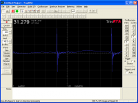
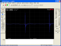
I've been poking around with measurements and came up with the attached a few minutes ago. These are close mic measurements of the impulse response on the driver with the 49600s remaining within their class A range. Left one's the 49713, right the 49990, and the wobbles between impulses are ambient noise. The RTA's running at 44.1kHz so there's presumably a fair amount aliasing of the post ringing. I'll remeasure at 96kHz when I get a chance but this calls for getting a decent scope on the driver leads and that's gear I don't have handy. I can, however, easily fish around to see if it's a bypassing issue by varying the signal level, shortening up the zip cord to the driver to reduce the capactive loading from something like 100pF to 30pF, stuffing the bulk caps, or tacking on additional 100nFs and 3.3uFs.
Attachments
Yes, what you're saying makes sense to me in a classical sense. However my working hypothesis is that RF ingress is the main villain in regards sound quality, which is why its so hard to pin down. Besides my own experience of grounding changes, there is some anecdotal evidence of low noise opamps being susceptible to RF. I think it was Ed Simon over on the Blowtorch thread who recently recommended a series air-cored inductor to the opamp input because RF was affecting his measurements. Walt Jung (or was it Jan Didden?) took out an AD797 from his low noise power supply and substituted a JFET one because of the former's extreme RF susceptibility in that particular application.
The key difference to my mind between your 49713 and 49990 is in the input stage - the latter is so low noise it can only have an undegenerated LTP with an extremely narrow linear differential input voltage range, ripe for RF aggravation.
The key difference to my mind between your 49713 and 49990 is in the input stage - the latter is so low noise it can only have an undegenerated LTP with an extremely narrow linear differential input voltage range, ripe for RF aggravation.
Why a resistor across cdom cap are bad ?
Hi GaetanI've ask this question because Douglas Self, in his book Audio Power Amplifier Design Handbook 5th edition, suggest to put a 100k to 500k resistor across the vas cdom cap to reduce the vas gain.
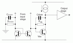
I can think of two issues. Firstly, it reduces vas gain so there is less global feedback to correct distortion. However it also reduces vas output impedance, which reduces distortion of the vas and output stage. The final result is still a bit more distortion, but not too bad.
The second issue is power supply rejection. With that type of vas the output voltage is relative to the negative supply voltage, so any ripple voltage on the negative supply rail is also on the output. Global feedback reduces this, but if feedback is reduced with a resistor across Cdom, PSRR will be worse.
The PSRR can be fixed by adding an extra capacitor and resistor as shown below with Cpsrr = Cdom and Rpsrr = Rnfb. Even without the resistors, adding the extra capacitor may be a good idea.
I like the idea of doing it like this as it allows a wide open-loop bandwidth.
Regards - Godfrey
Attachments
From a quick look at your layout, it does look like R3's grounding could be the culprit. In my experience the gain/feedback resistors do need their own clean ground back to the star earth.
That certainly is true for a single-ended design as ground currents in the feedback ground connection will introduce "crap" (yes, that's the technical term) into the amp input via the feedback network. However, this is a differential amplifier. The feedback should be taken across the load. The differential amp sets up a voltage difference across the load that depends entirely on the voltage difference between the (+) and (-) inputs of the amp. The output voltage is not referenced to ground at all (assuming high CMRR anyway). Hence, this circuit should be immune to ground bounce as laid out.
However my working hypothesis is that RF ingress is the main villain in regards sound quality, which is why its so hard to pin down. Besides my own experience of grounding changes, there is some anecdotal evidence of low noise opamps being susceptible to RF.
The key difference to my mind between your 49713 and 49990 is in the input stage - the latter is so low noise it can only have an undegenerated LTP with an extremely narrow linear differential input voltage range, ripe for RF aggravation.
RF interference in op-amps is very real. I wish I still had the oscilloscope shot I saw a few years ago. It showed the output voltage of two different op-amps, both in unity gain configuration. The inputs to the amps was grounded. So you'd expect a solid line on the o'scope of about +/-Vos, where Vos is the input voltage of the op-amp, right... Well... Next to the lab setup was a GSM cell phone. Then someone dialed the cell phone... One op-amp just went ape scat and showed a huge change in Vos. The other - LMV851, I think it was - showed hardly any change at all. The LMV851 is "EMI hardened", i.e. designed to withstand RF interference without significant shifts in performance. LMP2021 is another example of this.
The reason behind the Vos changes is that the RF is rectified by the various diode junctions (MOS, BJT junctions) and ends up as DC in the circuit. Adding some filtering on the amp inputs certainly makes sense. Many people use input caps to ground...
Now whether two amps sound differently because one is more susceptible to RF interference, I don't know. With the high GBP op-amps, that's certainly a valid concern. But I don't see any reason why one wouldn't be able to design an amp that's fairly RF immune with proper input and output filtering, careful layout, shielding, etc. Just keep in mind that it's not DC/audio anymore. It's RF design... 🙂
~Tom
The output voltage is not referenced to ground at all (assuming high CMRR anyway). Hence, this circuit should be immune to ground bounce as laid out.
Yet in similar configurations, I hear improvements in sound when grounds are cleaned up. So I accept your 'classical' arguments here, but they don't explain the sound quality differences. Perhaps the assumption of high enough CMRR when extended into VHF territory doesn't apply. Certainly I've never seen an opamp datasheet showing decent CMRR into 100MHz territory.
RF interference in op-amps is very real. I wish I still had the oscilloscope shot I saw a few years ago. It showed the output voltage of two different op-amps, both in unity gain configuration. The inputs to the amps was grounded. So you'd expect a solid line on the o'scope of about +/-Vos, where Vos is the input voltage of the op-amp, right... Well... Next to the lab setup was a GSM cell phone. Then someone dialed the cell phone... One op-amp just went ape scat and showed a huge change in Vos.
These are the gross RF effects I hear when my cell starts ringing or I receive an sms. But in audio I think there must be low-level effects just from the ambient airborne 'crap' when wires are long enough to collect it (as is the case for screens of interconnects).
The reason behind the Vos changes is that the RF is rectified by the various diode junctions (MOS, BJT junctions) and ends up as DC in the circuit. Adding some filtering on the amp inputs certainly makes sense. Many people use input caps to ground...
... and some just assume that the ground they used as a sink is a clean one. Often, its not at RF frequencies unless they have a good groundplane. So a cap to a dirty ground can make matters even worse.
But I don't see any reason why one wouldn't be able to design an amp that's fairly RF immune with proper input and output filtering, careful layout, shielding, etc. Just keep in mind that it's not DC/audio anymore. It's RF design... 🙂
Agreed, and maybe (to me at least) explains why so much consumer audio sounds a tad crap. RF designers probably earn more doing real RF design.😀
National has some special process tricks to reduce the sensitivity to emi/rfi. That is also one of the virtues of the venerable Signetics/Phillips 5534.
The filter stuff on the input and output of the amp to deal with RFI can do major damage to the audio signal.
The filter stuff on the input and output of the amp to deal with RFI can do major damage to the audio signal.
Looking carefully at the circuit I realized there are a few important questions to be resolved-
First the source signal, is it AC or DC coupled? (probably DC I would guess)
What is the source impedance?
Finally have you looked at the DC levels on the inputs?
The two opamps will have a different input bias currents and the lower noise one may well have a lot higher input bias current, since the bias current compensator circuits used add noise and may well have been dispensed with on that chip.
Source is a Focusrite Saffire 40; while ohming out the board is rather tricky I would assume the usual balanced pro audio buffer, which would be around 100 ohm source impedance. DC levels are fine and, yes, it's DC coupled. Input biases are the other way around; the datasheets are linked above if you want details but Ib is 30nA on the 49990 and 1.8uA on the 49713 (typ). While we're on the subject of 49990 performance, I get the floor of my test gear back measuring the 49990 channel---that's between -90 and -110dB depending on the test---up to 2V in. Above 2V the 49600 starts to clip on my loads and I haven't bothered to probe the 49990 output. Personally I wouldin't consider +/-2V an "extremely narrow" range, but to each their own.
However, I've lost repro. Repeats of measurements which showed differences yesterday evening show no difference tonight and I'm getting 0% discrimination on subjective A/B. Same board, cabling, connectors, supplies, moble phones around in the same locations and on/off states (not that I've seen any sign of RF coupling in the usual orientation testing or measured differences tonight with my mobile on and sitting next to the board), etc. I had consistent repro for four days before bumping this thread, so I'm seriously scratching my head here---nobody leaves their microwave on for four days straight and cell channel assignments change more often than that too. Check back the next time the moon's in first quarter. 😛
However, I've lost repro. Repeats of measurements which showed differences yesterday evening show no difference tonight and I'm getting 0% discrimination on subjective A/B. Same board, cabling, connectors, supplies, moble phones around in the same locations and on/off states (not that I've seen any sign of RF coupling in the usual orientation testing or measured differences tonight with my mobile on and sitting next to the board), etc. I had consistent repro for four days before bumping this thread, so I'm seriously scratching my head here---nobody leaves their microwave on for four days straight and cell channel assignments change more often than that too. Check back the next time the moon's in first quarter. 😛
Personally I wouldin't consider +/-2V an "extremely narrow" range, but to each their own.
If this is an allusion to one of my earlier comments, I agree that +/- 2V is by no means an extremely narrow range. That's not what I was talking about there. 😀
- Status
- Not open for further replies.
- Home
- Amplifiers
- Solid State
- Slew rate calculations - how much do I need?