Common base VAS can be made to work, but the wider FR means compensation must be tight. Furthermore, you no long have two points in antiphase, C and B, and so you must make the equivalent of the base from the drone side of the LTP, which is no bad thing.
It also makes the biasing of the VAS critical, since the base, not the emitter, determines its operating point. But it can be done.
Andrew, common base is a configuration for a single transistor. Cascode is a configuration for two transistors.
Cheers,
Hugh
It also makes the biasing of the VAS critical, since the base, not the emitter, determines its operating point. But it can be done.
Andrew, common base is a configuration for a single transistor. Cascode is a configuration for two transistors.
Cheers,
Hugh
Greg,
Transistors suitable for voltage amplification are characterized by low Icmax, typically 100mA (their most linear region being at 5-10 mA) and small Cob, below 5pF. They also have some "hidden" properties.
I expect the Cob of BD139 and MJE340 to be around 50pF, which can easily increase 100 times dynamically. These devices have a pitiful bandwidth and develop severe distortion.
Yes, you have said that and I have said that they do not belong to the list. As a replacement, it would be possible to make the list more complete.WARNING: Some of the more generic transistors (e.g. BD139 and MJE340) have incomplete datasheets and also have multiple manufacturers with varying specifications. Use caution when selecting these components.
Transistors suitable for voltage amplification are characterized by low Icmax, typically 100mA (their most linear region being at 5-10 mA) and small Cob, below 5pF. They also have some "hidden" properties.
I expect the Cob of BD139 and MJE340 to be around 50pF, which can easily increase 100 times dynamically. These devices have a pitiful bandwidth and develop severe distortion.
brand new (to me) topology and maybe actually new
Have never seen the circuit from the idea inspired by the other posters. Thanks again all! Simulation results were just plain astonishing using 2N2222A 2N2905A transistors in the sim. 80dB of open loop gain and set up as an op amp nominal gain of 20dB gave -3dB at 21MHz and 105 degrees of phase margin at unity gain. Of course there is loop gain error as open loop is only 80dB as many understand. Sim gain is 18.4dB. Well uncalibrated sims have problems as we all know. As a starting point though this seems really interesting. Will post the actual test results from the real circuit here I guess unless someone has a better thread to suggest.
As far as "nothing new" suppose that is surely a matter of literature research and the possibility there is an opportunity for a new design.
Thanks everyone again for inspiration!🙂🙂
sumaudioguy,
I wonder what it is, because there´s nothing left to invent.
😀
Have never seen the circuit from the idea inspired by the other posters. Thanks again all! Simulation results were just plain astonishing using 2N2222A 2N2905A transistors in the sim. 80dB of open loop gain and set up as an op amp nominal gain of 20dB gave -3dB at 21MHz and 105 degrees of phase margin at unity gain. Of course there is loop gain error as open loop is only 80dB as many understand. Sim gain is 18.4dB. Well uncalibrated sims have problems as we all know. As a starting point though this seems really interesting. Will post the actual test results from the real circuit here I guess unless someone has a better thread to suggest.
As far as "nothing new" suppose that is surely a matter of literature research and the possibility there is an opportunity for a new design.
Thanks everyone again for inspiration!🙂🙂
Last edited:
Common base VAS can be made to work, but the wider FR means compensation must be tight. Furthermore, you no long have two points in antiphase, C and B, and so you must make the equivalent of the base from the drone side of the LTP, which is no bad thing.
It also makes the biasing of the VAS critical, since the base, not the emitter, determines its operating point. But it can be done.
Andrew, common base is a configuration for a single transistor. Cascode is a configuration for two transistors.
To me, a common base is a transistor circuit where the emitter is driven by a current source. Whether this is the input signal source or the dependent current source of another transistor, i e the collector or drain, it doesn’t matter. If you look at the voltage gain device of a cascode, it is the second transistor that provides this. Of course the Z of the input must be lower to drive the emitter (source) of the cascode transistor than that for common emitter (source) amplifier. I find using the cascode for a balanced circuit (both sides have the same output Z) works very well provided it is driving a fairly high impedance. A single cascode works well also, if implemented properly.
Cascode, in terms of propagation delay, is one stage. Big advantage for a cascode, in that the current amplifier can be small signal and have low Vceo like 25V, with Hfe >400. These parts exist and are quite cheap. The high Hfe eliminates the need for a VAS buffer.😉 Choose the devices appropriately, low Vceo high gain, high Ft device for the current amplifier, and high Vceo, gain irrelevant, low Cob for the voltage gain device. The cascode voltage source should appear as 'ideal' to the base (gate) of the cascode transistor relative to the base current required. I think because people's misunderstanding of the idea foments animosity towards using a cascode VAS. That and the fact that a higher rail voltage supply required introduces a bit more circuit complexity. If your up for all that, without a doubt cascode, or common base (gate) is the way to go, IMHO.
Kanwar,
Nice circuit, I tried it in single end, worked fine, but I found that precisely for reasons Edmond identifies, it did not offer particularly good offset control because of wandering collector current.
The secret to stability was control over the loop gain with THAT resistor between the RC emitters (along with LTP degeneration). That was the best way to control the wayward high gain of the RC I have yet seen. But man, is that configuration fast!
Hugh
Greg,
Yes, you have said that and I have said that they do not belong to the list. As a replacement, it would be possible to make the list more complete.
Transistors suitable for voltage amplification are characterized by low Icmax, typically 100mA (their most linear region being at 5-10 mA) and small Cob, below 5pF. They also have some "hidden" properties.
I expect the Cob of BD139 and MJE340 to be around 50pF, which can easily increase 100 times dynamically. These devices have a pitiful bandwidth and develop severe distortion.
Hello
BD139 never give me best sound for a VAS, even for driver it's a bit slowish, so I use it for vbe multiplier.
Bye
Gaetan
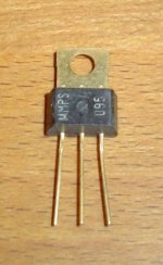
MPS-U60 and U10 the most obsolete of them all.
Ah, but they are Sooooo pretty and goldy.
Oh Oh, i've got it, how about a 2.5pF Ccb, 100K hFe darlington MPSU45/95 Vas ?

Attachments
How-do,
not the other way round ?
(if NOS retail price is an indication of obsoleteness, check out the MPS-U95 offerings )
not the other way round ?
(if NOS retail price is an indication of obsoleteness, check out the MPS-U95 offerings
)Kanwar,
Nice circuit, I tried it in single end, worked fine, but I found that precisely for reasons Edmond identifies, it did not offer particularly good offset control because of wandering collector current.
The secret to stability was control over the loop gain with THAT resistor between the RC emitters (along with LTP degeneration). That was the best way to control the wayward high gain of the RC I have yet seen. But man, is that configuration fast!
Hugh
Hugh,
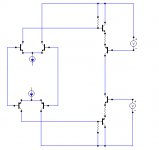
The offset stability was achieved by placing the emitter resistor between both emitters of pnp+npn combo pair.Besides that LTP degeneration was also used around 150ohms on both differentials. RC networks were used in parallel with both collector resistors to reduce gain at high frequencies.
Its main advantage is Extended power bandwidth and very less phase shift on high frequencies. Slew rate was in excess of 150V/us. PSRR also increased considerably.
Kanwar
Aha, Kanwar,
you put numbers to my observations, thank you......
Have you tried a singleton input stage? That too has phase advantages......
Hugh
you put numbers to my observations, thank you......
Have you tried a singleton input stage? That too has phase advantages......
Hugh
Jacco,
looks can be deceiving, I once removed the top cover by chance and saw a large number of devices carefully designed for switching purposes lying everywhere. Made some changes and noticed a remarkable difference, so I thought that some kind of enhanced diffusion process must be used on these ones, could I be wrong?
looks can be deceiving, I once removed the top cover by chance and saw a large number of devices carefully designed for switching purposes lying everywhere. Made some changes and noticed a remarkable difference, so I thought that some kind of enhanced diffusion process must be used on these ones, could I be wrong?
Aha, Kanwar,
Have you tried a singleton input stage? That too has phase advantages......
Hugh
Hugh,
I never tried singleton[feedback at emitter] or single polarity differential in my amplifiers.........🙁
Kanwar
Hi Gaetan,
a Vbe multiplier acts as a constant voltage source; "speed" means a desirable low impedance over a wide frequency range.
a Vbe multiplier acts as a constant voltage source; "speed" means a desirable low impedance over a wide frequency range.
Kanwar,
there are some papers preaching a common collector stage between the transconductance and the transimpedance amplifier, but it has a poor theoretical bases (in my exceedingly humble view).
there are some papers preaching a common collector stage between the transconductance and the transimpedance amplifier, but it has a poor theoretical bases (in my exceedingly humble view).
Kanwar,
there are some papers preaching a common collector stage between the transconductance and the transimpedance amplifier, but it has a poor theoretical bases (in my exceedingly humble view).
Do you have any papers or links showing this?🙂
looks can be deceiving
Popping the hood is like Window Shopping, you never know what you get untill you bring it home.
- Home
- Amplifiers
- Solid State
- It's 2010 and what's your fav VAS transistor?