Salas, a 10R-3300u RC filter didn't make a difference. On average the measured noise was still 0.43nV/rtHz (at 1kHz).
Set aside the noise impact of the resistor, that would be a loop gain killer (appears AC parallel with the CCS).
The resistor can be ~10k ohm so does not cause the issues you mention. In fact it hardly matters where you place the servo--its a matter of choosing the correct authority and this will also minimise its noise contribution. If decoupling can't be as high as one wants add an RC filter as in your original schematic.
Samuel
Salas, a 10R-3300u RC filter didn't make a difference. On average the measured noise was still 0.43nV/rtHz (at 1kHz).
Looks like the CCS took care. Thanks.
Hi Ikoflexer,
As you already observed the J310 current source makes the DC operating point quite sensitive to component values, temperature etc. The input stage acts as a current source, so does the drain current source J310. So in fact both current sources are fighting each other and the weakest (the one with the lowest output impedance) will "give in". So fundamentally this solution is flawed, though in practice it could work due the current source "saturation" already mentioned by Samuel and Syn08.
If I've understood correctly, you tried the J310 current source to improve PSRR. May I suggest another approach to improve PSRR?
The PSRR in the circuit with the 150 Ohm drain resistor is poor due to the fact that the DC servo (opamp U2) refers the LNA output signal to ground. This ground referred control signal is fed into the + input of the 1st opamp, while the - input of this opamp refers to the power supply through the 150 Ohm drain resistor of the input stage. Now any noise on power supply or ground is directly imposed on the difference between + and - input, and amplified by a huge amount of loopgain of U1.
The trick for good PSRR should be to refer the DC servo control signal to the power supply too. My proposal would be to simply replicate a scaled version of the input stage, say 1/9 (so 1 JFET) and a 9x higher drain resistor (say 9*150 Ohm) to the power supply. Now the input of this replica branch can be driven from the non-inverting DC-servo of your last post above. The 9*150 Ohm resistor can be connected between supply and the + input of the 1st opamp. This way, both + and - input are referred to the power supply, so any disturbance is nullified on the OpAmp inputs. Basically the same ripple occurs on the drain of the input JFETS and the replica branch, having a net effect of 0. The non-inverting DC-servo controls the LNA output offset voltage though the replica JFET gate. (ideally both branches would have equal components, but that's power hungry and high component count)
This approach requires slightly more components than syn08's HPS5.1 solution with decoupling cap, but works from DC to high frequency.
Worth a try?

Hi Jeepee,
I thought the first stage would have the most impact as far as psrr goes, but I will try your suggestion first in the simulator, thanks!
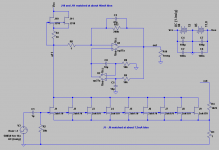
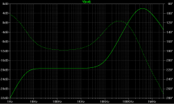
Jeepee, is this what you mean or have I misunderstood? The frequency response with R5 = 1350R is very poor (low gain) up to about 80kHz. A value of 200R makes it almost OK.
I thought the first stage would have the most impact as far as psrr goes, but I will try your suggestion first in the simulator, thanks!
Jeepee, is this what you mean or have I misunderstood? The frequency response with R5 = 1350R is very poor (low gain) up to about 80kHz. A value of 200R makes it almost OK.
Attachments
I just looked up an IEEE paper by Scott Wurcer where he mentioned the presence of gate series resistance in JFETs and according noise contribution and deviation from Ziel's estimate. Scott, do you have any idea what this resistance might be in a device like the 2SK170 or BF862?
Samuel
This contribution is very small for these FET's and difficult to extract by noise measurement alone. Typical contact resistance is only a few Ohms but at these levels 4-6 Ohms in each the gate and source should be detectible. Someone would need to make a real project out of this and average a LOT of noise data. You are talking about verifying something like a theoretical value of .66nV and actual .8nv (just making up numbers). You can see how very small differences in measurement can give large differences in calculated R's. Here (my made up example) .68 vs .66 nV is 12 vs 10 Ohms parasitic.
Before I forget, this is probably all moot because the factor that you multiply the 1/gm of the FET to get the theoretical noise is not based on physical constants. The usual ~2/3 is from integration of the ideal Shockley Fet model and is simply from fractional power law exponents like tube equations. This is not the case for these short channel devices. See Cobbold and/or Van der Zeil.
Last edited:
Hi Ikoflexer,
that's indeed the circuit I described.
From your statement I gather that the PSRR is still poor with 9*150 Ohm? With the 200 Ohm you mentioned, what PSRR did you achieve? So it seems you have to spend the current and make both resistors the same value; 150 Ohm each? With this topology good PSRR is a "balancing act" between + and - branch...
Edit: looks like the pole of the DC-serve of quite high @ 10k/10uF. The JFET provides extra loopgain, shifting the closed loop DC-servo pole to higher frequencies. You might want to try 1MOhm for R5/R9. Was this your remark about "The frequency response with R5 = 1350R is very poor (low gain) up to about 80kHz." ?
Last edited:
Hi Ikoflexer,
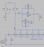
Can you try to make R7 = 9*1 Ohm and R6 = 9*150 Ohm. That way the replica branch is an exact scaled copy. Maybe you should also put a 9*200kOhm resistor from the + input of U1 to ground to mimic R12 (and a 47pF/9 in parallel to mimic C3). [afterall the DC-servo forces U1 output to 0V, so for DC R12 is from - input to 0V].
PS: what's the DC voltage on node a11?
Last edited:
Hi Ikoflexer,
good to hear you got the circuit working...
I just realised the replica can be even better approximated by using an inverting DC-servo integrator and a 9*1025 (9*R4) resistor towards the source of J10, while it's gate is pulled to ground. That way the DC-servo feedback is a 9x scaled up version of the main LNA feedback loop. Using J10 as a common gate stage (control via the source) is non-inverting, so the DC-servo needs to be of the inverting type for proper sign around the DC feedback loop.
PS: I realised I made an error in my previous post (corrected in the mean time), should have been: R11 = 9*R12= 9*200k, C9 = C3/9 = 47p/9.
This might be the reason why the PSSR is worse than your 1st result...
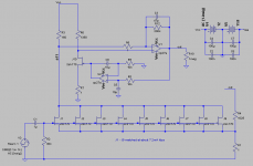
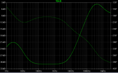
OK, see attached for updated schematic and psrr plot. The frequency response is good (not attached).
The DC voltage at node a11 is 2.92V.
For better high freq PSRR, try cascoding bank of sk170's into a BC337. Also
put a cap across R6, as it is only used as a servoed voltage reference.
cheers
Terry
Thanks Terry, but adding a cap across R6 worsened the PSRR. Also, have you had a look at syn08's HPS 5.1?
http://www.diyaudio.com/forums/soli...te-low-noise-amplifier-lna-5.html#post2182865
Is that what you mean (cascode)? If so, I have tried that.
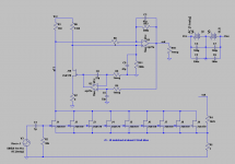
There's this other simple ccs (attached) that raised the open loop gain of the first age to over 60dB and in simulation it works fine, but doesn't seem to work at all in the real world. 🙁
In any case, at the moment the circuit with the J310 CCS and no PSRR works best (on batteries) and measures at 0.43nV/rtHz. It puzzles me how syn08 could so easily get 0.3nV/rtHz. 🙂
OK, so please, who else has 60dB preamps with 0.3nV/rtHz? What's the circuit you're using?
http://www.diyaudio.com/forums/soli...te-low-noise-amplifier-lna-5.html#post2182865
Is that what you mean (cascode)? If so, I have tried that.
There's this other simple ccs (attached) that raised the open loop gain of the first age to over 60dB and in simulation it works fine, but doesn't seem to work at all in the real world. 🙁
In any case, at the moment the circuit with the J310 CCS and no PSRR works best (on batteries) and measures at 0.43nV/rtHz. It puzzles me how syn08 could so easily get 0.3nV/rtHz. 🙂
OK, so please, who else has 60dB preamps with 0.3nV/rtHz? What's the circuit you're using?
Attachments
If I may contribute, current source load and undersized coupling cap are two obvious problems, which keep it more noisy than it could be.
ikoflexer, you need a different servo connection. If you're very interest I can sketch something but I need some time.
Samuel
Samuel
There's this other simple ccs (attached) that raised the open loop gain of the first age to over 60dB and in simulation it works fine, but doesn't seem to work at all in the real world. 🙁
Hi Ikoflexer, this topology still has the "fighting" current sources. In the simulator you can "tweak" it to work, but not in real life.
A solution could be to slave the operating point of the top current source to the natural operating point of the input stage JFET's. The input stage drain current is set by the source resistor of 1 Ohm and the gate pulled to ground. This results in a certain drain current Id (9*7.2mA in your schematic). Now the top current source, for example the current mirror in your post 294, needs to supply exactly that Id to the input JFET's. This is an equilibrium situation, where the voltage on node a11 hovers somewhere midway between supply and ground potential. A little bit more current from the top and bang node a11 sits near supply potential.A little less current and it sits near ground potential. You've already seen this stage has an openloop gain of 60dB, so the slightest inbalance and off it goes. So you need a mechanism to maintain the equilibrium; the DC-servo can be used for this.
Connect the + input of U1 to a fixed voltage, e.g. 3V referred to ground. A non-inverting DC-servo drives the gate of a JFET with 9 Ohm in the source (1/9 the input stage). Connect the drain of this JFET to the input of the bipolar current mirror Q2. Now a closed loop is formed that keeps the fighting current sources in check, maintains 3V on the drain of the input JFET's and delivers a 0V DC output signal. You'll probably want to apply some degeneration resistors in the emitters of the PNP's to keep the noise down. Say 9*150 for Q2 and 150 Ohm for Q1. This also provides a nice 1:9 mirror ratio in order to keep the control current reasonable. [maybe you have to increase the supply voltage by +2V to allow for a reasonable Vce for Q1].
The 3V reference voltage source for U1's + input can be created with a current source from the supply (use your J310 FET current source) and 2 LED's to ground. Now all nodes a shielded from the supply by current sources, so I expect the PSRR to be quite good.
As for the noise barrier you try to break, the current noise contribution of the 150 resistor, the J310 current source or your BD140 current mirror may not be neglected. The current noise of this drain "current source" (resistor, J310, mirror) appears in parallel to the precious drain current noise of the JFET's and "sees" the same amplification by the transimpedance stage (U1/R12). The higher the drain resistor, the better (also holds for the above proposed degeneration resistors in the current mirror). So a higher supply is probably the only way to further reduce the noise. Or, as Samuel suggested earlier, bias the JFET's at a lower current and use higher drain resistor. It will be a trade of between Id, gm and Rdrain.
Hope this helps to break the noise barrier

Last edited:
John, I understand what you say about the coupling cap, but I don't know what you mean about noise from the CCS load. Glad if you can pitch in.
Samuel and Jeepee, your willingness to help me is very much appreciated! This being said, I don't know if it's warranted to come up with a servo for the CCS in post 294. Last night the last experiment I did was to use the BD140 current mirror with 9x2sk170v (90mA Id) AC coupled via a 4uF to a OP07 (I happen to have a bunch of these on hand). The OP07 was simply connected as an inverting amp, with 1R on -IN and 100K feedback resistor. The DC component on the output of the opamp was a few millivolts, and from it a 1K resistor feedback to the jfet source. The open loop gain of the first stage was greater than 60dB, and I was hopeful with that. But the noise measured at about 4nV/rtHz.
So what I don't understand well is why the BD140 current mirror would have such higher noise, whereas the simple 2xJ310 CCS achieved the lowest noise.
Jeepee, I'm not dismissing your suggestion, just want to put these facts out for discussion.
- Home
- Amplifiers
- Solid State
- Simple 60dB discrete low noise amplifier (lna)