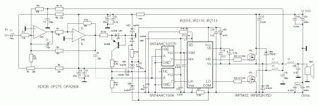
Somehow strange it turns out😕, if on an amplifier input will be 2V that at factor of strengthening K=20 - on an exit should be 40V but how it is possible if these limiting diodes do not allow be formed potential differences between inputs opamp more than 0,7V I can not to understand why they will not limit a signal.
Please do not mix together the AMPLIFIER inputs (before R2) and OPAMP inputs (after R2) - they have very different voltages! If on an amplifier input will be +2V, then on an exit will be -40V, and voltage drop on R2 and R3+R18 will compensate each other and at OPAMP inputs there will be near zero RMS voltage...
Usual OPAMP (operational amplifier, TL081) has amplification coefficient more than 100 000. Can you imagine that 0.7V at opamp inputs are amplified 100 000 times? This should be 0.7V * 100 000=70 000 Volts then or opamp will simply clip it. Under normal operation conditions there is not more than few millivolts at OPAMP inputs, that is why the diodes do NOT limit anything...
Last edited:
ОК, now it is more clear, but what maximum the entrance signal without clip can strengthen tl081 at a +/-15V PSU voltage? Has noticed one more "feature" in the amplifier, in the changed scheme it starts to work only after giving on an input of a small signal, it can is necessary to lower the added resistor to 100K?Please do not mix together the AMPLIFIER inputs (before R2) and OPAMP inputs (after R2) - they have very different voltages! If on an amplifier input will be +2V, then on an exit will be -40V, and voltage drop on R2 and R3+R18 will compensate each other and at OPAMP inputs there will be near zero RMS voltage...
Usual OPAMP (operational amplifier, TL081) has amplification coefficient more than 100 000. Can you imagine that 0.7V at opamp inputs are amplified 100 000 times? This should be 0.7V * 100 000=70 000 Volts then or opamp will simply clip it. Under normal operation conditions there is not more than few millivolts at OPAMP inputs, that is why the diodes do NOT limit anything...
Last edited:
Hi,
I missed a few episodes🙂
Reasons of "81Bas" is correct.
Clip signal directly on pin diodes.(one protection for OpAmp only)
In practice, what problems you have on the amplifier?
you want clipped signal Input?
Regards
I missed a few episodes🙂
Reasons of "81Bas" is correct.
Clip signal directly on pin diodes.(one protection for OpAmp only)
In practice, what problems you have on the amplifier?
you want clipped signal Input?
Regards
Hi, 81bas has helped to understand with entrance diodes and sensitivity of the amplifier. At present there were two problems: start occurs from an entrance signal and there was a deenergizing impulse (still in it was not engaged).Hi,
I missed a few episodes🙂
Reasons of "81Bas" is correct.
Clip signal directly on pin diodes.(one protection for OpAmp only)
In practice, what problems you have on the amplifier?
you want clipped signal Input?
Regards
ОК, now it is more clear, but what maximum the entrance signal without clip can strengthen tl081 at a +/-15V PSU voltage? Has noticed one more "feature" in the amplifier, in the changed scheme it starts to work only after giving on an input of a small signal, it can is necessary to lower the added resistor to 100K?
This is why the startup circuit on T2 was here 😉
Measure a voltage on C13 when the amp is 'not working' (before giving input signal). If it is less than 8-10 volts, then it is needed to reduce the resistor between Vb and +65V. Also, if the resistor is too small, then it can produce too high voltage on C13 and damage the driver. To be safe, simply put a 15V Zener diode (стабилитрон) parallel to C13.
Also, if this will not help, then it will be needed to insert delayed SD signal for IR2110.
Not good idea, put zener and low res).
replace T2, but decrease base-capacitor for minimum sbalanced necessary for start.
I think simple relay is good also for protection(DC-Offest) on Speakers.
replace T2, but decrease base-capacitor for minimum sbalanced necessary for start.
I think simple relay is good also for protection(DC-Offest) on Speakers.
Last edited:
Not good idea, put zener and low res).
replace T2, but decrease base-capacitor for minimum sbalanced time.
which 'low res' did you mean? 100K is low res? 😕
100K not to provide the current necessary.
when totempole (ir21) switch-on, voltage drops immediately.( at threshold voltage of internal UVLO).
Res (I Used 47K)is only for help
when totempole (ir21) switch-on, voltage drops immediately.( at threshold voltage of internal UVLO).
Res (I Used 47K)is only for help
Last edited:
With it all is clear😉This is why the startup circuit on T2 was here 😉
Measure a voltage on C13 when the amp is 'not working' (before giving input signal). If it is less than 8-10 volts, then it is needed to reduce the resistor between Vb and +65V. Also, if the resistor is too small, then it can produce too high voltage on C13 and damage the driver. To be safe, simply put a 15V Zener diode (стабилитрон) parallel to C13.
How delayed SD signal for IR2110 can promote amplifier start?Also, if this will not help, then it will be needed to insert delayed SD signal for IR2110.
not start.With it all is clear😉
How delayed SD signal for IR2110 can promote amplifier start?
for starting, is necessary OpAmp exceed the threshold logic input to next stage.(or T2 force pwm to unbalanced )
Last edited:
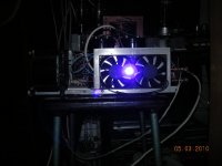
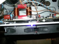
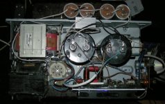
Amplifier photo 😎
Attachments
Last edited:
How delayed SD signal for IR2110 can promote amplifier start?
If you look at the IR2110 block diagram, you will see, that the high side driver is receiveing only short pulses to enable or disable HOUT pin from PULSE GEN circuit. And if the high side is not powered up yet (C13 in your schematic is not charged yet) and HIN pin becomes high, then yet NOT POWERED high side will simply ignore the enabling pulse. And after C13 is charged to working voltage, the high side will still stay not enabled, because the enabling pulse was lost previously.
So if we will enable SD signal at startup of the amp, and if we will disable SD signal with some delay after C13 is charged, then high side enabling pulse will be sent correctly and amp will start to work...
Huh, so much words... 😀
🙂..very good but.....(1) active pulse on SD(low-hi-low) not used all amplifiers.
(2) Internal UVLO predominates all function of IR21xx.
Very interesting and deep idea... As it is possible to combine this delay with the deenergizing scheme?If you look at the IR2110 block diagram, you will see, that the high side driver is receiveing only short pulses to enable or disable HOUT pin from PULSE GEN circuit. And if the high side is not powered up yet (C13 in your schematic is not charged yet) and HIN pin becomes high, then yet NOT POWERED high side will simply ignore the enabling pulse. And after C13 is charged to working voltage, the high side will still stay not enabled, because the enabling pulse was lost previously.
So if we will enable SD signal at startup of the amp, and if we will disable SD signal with some delay after C13 is charged, then high side enabling pulse will be sent correctly and amp will start to work...
Huh, so much words... 😀
Very interesting and deep idea... As it is possible to combine this delay with the deenergizing scheme?
I think yes 😉
To prove this theory, you can simply connect SD pin via 50K resistor to COM pin, and connect SD pin via 10uF cap to pin 3 (15V Vcc of driver). This should produce a long SD signal at startup. If this will work, then I can try to paint a circuit for startup SD delay and deenergizing...
Also, have you tried to reduce the 200K resistor to 100K? (between +65V and Vb pin?)
Work on the amplifier I will continue a bit later, has found the similar scheme in it SD it is connected with COM through the resistor 10K (probably for delay creation) as in it there is a chain of diodes VD2-VD5 from which also arrives the signal on SD how you think in such a way is formed smooth deenergizing?It would be very interesting to see your variant of start / smooth deenergizing with reference to my scheme.I think yes 😉
To prove this theory, you can simply connect SD pin via 50K resistor to COM pin, and connect SD pin via 10uF cap to pin 3 (15V Vcc of driver). This should produce a long SD signal at startup. If this will work, then I can try to paint a circuit for startup SD delay and deenergizing...
Also, have you tried to reduce the 200K resistor to 100K? (between +65V and Vb pin?)
Attachments
Last edited:
Hi,
My post "LM339" circuit solved two problems.
startup and no"PUP" when switch-off psu.
You have tested?
My post "LM339" circuit solved two problems.
startup and no"PUP" when switch-off psu.
You have tested?
Yet did not do, you could describe more in detail algorithm of work of your scheme, and also what delay it provides at inclusion? You tried it to test?Hi,
My post "LM339" circuit solved two problems.
startup and no"PUP" when switch-off psu.
You have tested?
- Status
- Not open for further replies.
- Home
- Amplifiers
- Class D
- Self-oscillating class D amplifier