Try making R1 68 ohms. It shouldn't be zero, I would avoid that.
I don't quite understand the overshoot issue. The Allison itself shouldn't have overshoot with so much compensation, but anything's possible. I also don't have any experience with using chips or opamps, and that odd "compensation" pin is quite new to me. Is it possible it could be a wiring error?
- keantoken
Last edited:
I'd ditch base stoppers on Q2 and Q3. The way those transistors eat base current...
If you really worried, put a low low inductance - yet lossy at RF, type ferrite bead.
If you really worried, put a low low inductance - yet lossy at RF, type ferrite bead.
Is it possible it could be a wiring error?
- keantoken
Yesterday was one of those days... had Paul' A/B running at higher bias as described in prior note was trying to optimize the compensation cap value. Went to 68pf and it was not happy, or so I thought. Went back to 56pf, was getting square waves out from a sine in. Basically rebuilt the entire output stage, swapping out the diodes, Allison transistors, drivers, still no good. Wanting to verify that it was not the LMe49811, I hooked up the Allison output, it was doing the same thing, sometimes square waves, sometimes triangle waves. Tried all sorts of ground connections - I use a 10 ohm resistor to separate the signal ground from power ground. Finally moved the Zobel from the signal ground to the power ground, solved the problem immediately. Weird thing is, it had be set that way from months. So, all prior thinking is now in question. Were there really problems or was it this?
Anyway, now Paul's scheme doesn't overshoot, rather, it rounds the square wave off a lot at 20kHz. Didn't do much more than verify that it ran and then went to bed. I'll go back tonight and see if the variable bias runs 😱 and maybe take some measurements on Paul's scheme.
Ken L
I'd ditch base stoppers on Q2 and Q3. The way those transistors eat base current...
If you really worried, put a low low inductance - yet lossy at RF, type ferrite bead.
Ken,
Did you mean Q2/Q8 the 330r R2/R4? from Keantokens earlier post.
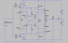
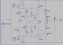
I've attached an updated version, and wouldn't you know, I have different device numbering... I've also shown my idea of how to implement compensation - have I done this correctly? I've also left off the two diodes between the Allison pair but will make the board to accomodate them trying it both ways.
As a last point, when I put a square wave throught the simulation I get overshoot and ringing. Have your tried this in simulation?
Ken L
Attachments
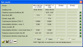
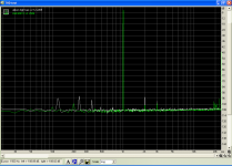
New results for the Allison A/B Paul's scheme with two of the four Re diodes removed and .22r Re's. With the grounding sorted out it measures well against the baseline of .0041 THD for the LME49811 alone. I tried one more test after saving the Test Results image - with the sound card ground moved to a different location and it dropped the THD to .0045. The driver transistors are 15032/33s. They are getting pretty hot - currently no heat sink on them.
Ken L
Ken L
Attachments
The attached schematic is basically the configuration from the test results shown in the prior post with the exception of R13. For the test R13 is set at 100r, to lower the temp and bias on the driver transistors Q1/Q5, I have simulated it at 500r - no change in the THD or FFT. It lowers the wattage by about half. Do you see any problems with this?
Ken L
Ken L
Attachments
You have the compensation set up right and I see nothing wrong with changing R13 the way you have. The point of R13 is to keep the drivers working in their more linear range, I might have set it too high.
And I believe Kenpeter means the 4.7 ohm resistors on the MJL's
- keantoken
And I believe Kenpeter means the 4.7 ohm resistors on the MJL's
- keantoken
keantoken,You have the compensation set up right and I see nothing wrong with changing R13 the way you have. The point of R13 is to keep the drivers working in their more linear range, I might have set it too high.
- keantoken
Are you looking at the VCE -Ic graph for the device - DC current gain hFE against the Collector current? Can you show me a spice output for this from the variable bias simulation? It would help me understand how R13 is set.
Ken L
On a similar topic, how did you set the values of R3/R4 in post 431?
After posting my schematic I ran the similuation and found that removing them degraded the performance, so, as you say, it must be the resistors at the bases of the MJL's that Ken Peter was refering to.
Ken L
After posting my schematic I ran the similuation and found that removing them degraded the performance, so, as you say, it must be the resistors at the bases of the MJL's that Ken Peter was refering to.
Ken L
I've attached an updated version (#444), - have I done this correctly?
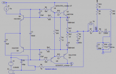
Uh, Q8 and Q9 appear shorted base to collector...
Q4 and Q8 starve the Darlingtons from ever seeing
more than half the bias voltage they would need to
turn on. So, I'm gonna guess drawing #444 is broke.
Getting rid of the shorts:
Emitters loads of Q4 and Q6 probably shoulda been
independantly CCS'ed or bootstrapped to the rails?
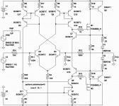
How about this?
Attachments
The prob with current drive from over and under (rather than between the emitters)
is that its darn near impossible to bootstrap for full output swing... I've simm'd a few
discrete variants of your op-amp circuit. Can't get closer than 5V to either rail with
enhancement MOSFETs. And bipolar Darlingtons want for much current, and rather
asymmetrically at that.
I prefer enhancement mosfet drives pulled up with bootstrap as-if fake CCS (Aleph).
But I can't get there from here, goin' round the outside. Allison sliding in the middle.
I'd need a whole separate set of higher rails just for the drives, not to be burning
output headroom for waste heat.
What you see here sims really "good?" As long you don't ask more than +/-20 out.
I mean, the distortion is absurdly low (low for one of my AB's) around +/-10 out...
But I won't rest till I got withinavolt of rail2rail, and gracefully compressed clipping.
This just doesn't get me to where I want to be (yet).
Attachments
Last edited:
Uh, Q8 and Q9 appear shorted base to collector...
Q4 and Q8 starve the Darlingtons from ever seeing
more than half the bias voltage they would need to
turn on. So, I'm gonna guess drawing #444 is broke.
Getting rid of the shorts:
Emitters loads of Q4 and Q6 probably shoulda been
independantly CCS'ed or bootstrapped to the rails?
The current loading of Q4 and Q6 is minimal because it really doesn't affect distortion or performance much. (after all, the signal is going out through two diodes)
Are you looking at the VCE -Ic graph for the device - DC current gain hFE against the Collector current? Can you show me a spice output for this from the variable bias simulation? It would help me understand how R13 is set.
On the 4793 datasheet, Hfe crests at around 60mA... This would be the optimal bias point, but that's a little hot and the device is so linear I don't think it matters that much anyways. What's most important is that the device has enough bias current that it won't turn off on current spikes. I'm pretty sure 500 ohms is fine here.
On a similar topic, how did you set the values of R3/R4 in post 431?
Q3 and Q4 need to pass lower current than Q6 and Q5 so that the voltage across the schottkeys can not be below zero. We can assume that the Vcb of Q5/6 is roughly .5V because of the darlingtons, and based on this we need to put less than 4.5mA through Q6 and Q5 (4.5 is half of 9ma) so .5/330=1.5mA. This should be safe.
- keantoken
The current loading of Q4 and Q6 is minimal because it really doesn't affect distortion or performance much.
His update with 330ohm rather than a dead short would probably work.
How well, I don't know? I havn't simm'd it.
330 ohms was my "updated" value... If we were using resistors instead of shottkeys, the loading here would be crucial to performance.
I can post the simulation files, if you want.
- keantoken
I can post the simulation files, if you want.
- keantoken
The prob with current drive from over and under (rather than between the emitters)
is that its darn near impossible to bootstrap for full output swing... I've simm'd a few
discrete variants of your op-amp circuit. Can't get closer than 5V to either rail with
enhancement MOSFETs. And bipolar Darlingtons want for much current, and rather
asymmetrically at that.
I prefer enhancement mosfet drives pulled up with bootstrap as-if fake CCS (Aleph).
But I can't get there from here, goin' round the outside. Allison sliding in the middle.
I'd need a whole separate set of higher rails just for the drives, not to be burning
output headroom for waste heat.
What you see here sims really "good?" As long you don't ask more than +/-20 out.
I mean, the distortion is absurdly low (low for one of my AB's) around +/-10 out...
But I won't rest till I got withinavolt of rail2rail, and gracefully compressed clipping.
This just doesn't get me to where I want to be (yet).
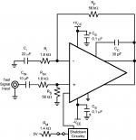
I haven't tried to run it from the center yet. I think it will work. It's how I test the LME49811 THD as shown in the National app. note. (1st image) But, how would I inject the signal between the emitters in keantoken's scheme?
Ken L
Attachments
You would have to chop R1 (in post 451) into 2 resistors, and add current sources at the collectors of Q8 and Q9. They could be bootstraps.
I'm sure it would work if you drive it from the center. The Allison likes this, I was only cautious at the beginning because I wasn't sure of the chip could do this, but obviously it can.
- keantoken
I'm sure it would work if you drive it from the center. The Allison likes this, I was only cautious at the beginning because I wasn't sure of the chip could do this, but obviously it can.
- keantoken
Last edited:
I just remembered this same thing and was getting back on-line to say that's why I didn't do it earlier, but, you beat me to it...You would have to chop R1 (in post 451) into 2 resistors, and add current sources at the collectors of Q8 and Q9. They could be bootstraps.
I'm sure it would work if you drive it from the center. The Allison likes this, I was only cautious at the beginning because I wasn't sure of the chip could do this, but obviously it can.
- keantoken
And here I raced home tonight and etched a new board... I'll get it running and then make some mods.
Ken L
Ken L
One modification that might help sound quality... A 22 ohm resistor across the output schottkeys. This keeps the MJL's from turning completely off. However, it will increase the heat. You might decide against it.
I can draw up a schematic for the emitter-driven version if you want.
- keantoken
I can draw up a schematic for the emitter-driven version if you want.
- keantoken
- Home
- Amplifiers
- Solid State
- Simulation Analysis of several unique Allison-based output stages.