Here is why it will not work well without source resistors. Let's look at Vgs = 4.5V and Vds > 10V. In that case, the drain current is:
For temperature = 25 Celsius, it is Ids = 0.6A.
For temperature = 150 Celsius, it is Ids = 25A.
That is not a reduction in current with increased temperature!
All the parallelled transistors have the same Vgs so the hottest one will work harder than the others. Drawing a load line and pointing at it is nonsense. It is current sharing that is the problem, nothing to do with the load line.
However, the BUZ9** transistors you mention on your page do not have this problem. They can be parallelled just fine without resistors.
Exactly.
It is impossible to support IRF240/9240 design by making reference to properties of lateral BUZ devices.
Thank you Federmann for your latest simulation presented!
Could also show a simulation with only gate voltage of both IRFP240 and IRFP9240 and output voltage of the amplifier, thank you!
Could also show a simulation with only gate voltage of both IRFP240 and IRFP9240 and output voltage of the amplifier, thank you!
Federman, please post somewhere .cir data for your "amplifier" (included used models), so we can talk about simulations of the same circuit. Maybee you are using Zener diodes with variable treshold voltage, new invention?
 I've been pulling personal stuff and what appear to be fights from other forums being dragged in here for several days. This is highly annoying. Any further personal attacks I pull out of here will result in Bin time. Criticize designs or technical thought, not people- basic rule.
Federman, please post somewhere .cir data for your "amplifier"
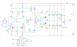
By the time we are waiting for the data, I have implemented the discussed output stage into another amplifier, which I believe can be used for evaluation of the output stage behaviour. First, let's normal operating conditions.
Attachments
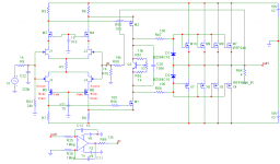
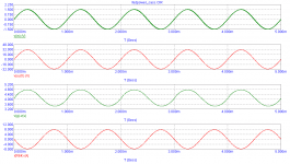
Supply voltage ± 91V. Sizes of resting currents
Burden 4Ω
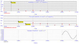
Burden 2Ω
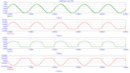
Burden 1Ω
Burden 100mΩ
Burden 10mΩ
An externally hosted image should be here but it was not working when we last tested it.
Burden 4Ω
An externally hosted image should be here but it was not working when we last tested it.
Burden 2Ω
An externally hosted image should be here but it was not working when we last tested it.
Burden 1Ω
An externally hosted image should be here but it was not working when we last tested it.
Burden 100mΩ
An externally hosted image should be here but it was not working when we last tested it.
Burden 10mΩ
An externally hosted image should be here but it was not working when we last tested it.
So, 30A current, 90V voltage, 2,7kW dissipation for 5 mosfets.You call it "protection"?? And Zener diodes are certainly not 10V types, as posted in original schematic, it is simply impossible. Post voltages across zeners..

You're right, it's just a demonstration.
When supply voltage is 91V output power:
1) 500W/8Ω. Zener diode must be selected so as to limit current to 12A (2.5 A * 5 or 3A * 4).
2) 1kW/4Ω. Zener diode must be selected as a transistor must be 8 or 10 pairs of 25A (2.5 A * 10 or 3A * 8).
When supply voltage is 91V output power:
1) 500W/8Ω. Zener diode must be selected so as to limit current to 12A (2.5 A * 5 or 3A * 4).
2) 1kW/4Ω. Zener diode must be selected as a transistor must be 8 or 10 pairs of 25A (2.5 A * 10 or 3A * 8).
An externally hosted image should be here but it was not working when we last tested it.
An externally hosted image should be here but it was not working when we last tested it.
Federmann, in opposite to you, I had build in last twenty years several hundred mosfet amps and I had in my hands several thousand mosfets...I have practical experiences, not only these f... simulations like you...Show to us practical results, not only these theoretical blables
Zener diode must be selected so as ...
I wonder if it is possible to make it so and to keep both linearity and protection. I am saying IT IS NOT.
Federmann, you argue here with people like Pavel Dudek (Upupa Epops) who has designed a lot of professional amplifiers that were sold in thousands, and with Ladislav Bunta (BV) who makes a living like an amplifier designer and producer, and again is commercially succesfull.
Contrary to that, you display some strange ideas, that are potentially hazardeous and dangerous for potential less experienced builders. You have no prototype, no sample. I must mention that, though I get a risk to be treated somehow. I hope there are some competent people who MUST see that.
Last edited:
I wonder if it is possible to make it so and to keep both linearity and protection. I am saying IT IS NOT.
Federmann, you argue here with people like Pavel Dudek (Upupa Epops) who has designed a lot of professional amplifiers that were sold in thousands, and with Ladislav Bunta (BV) who makes a living like an amplifier designer and producer, and again is commercially succesfull.
Contrary to that, you display some strange ideas, that are potentially hazardeous and dangerous for potential less experienced builders. You have no prototype, no sample. I must mentione that, though I get a risk to be treated somehow. I hope there are some competent people who MUST see that.
It seems that the big danger is the technically not-competent person who does not see whatever danger may exist.
It seems that the big danger is the technically not-competent person who does not see whatever danger may exist.
Exactly, you got it right.
I wonder if it is possible to make it so and to keep both linearity and protection. I am saying IT IS NOT.
I agree; it is NOT possible.
Overcurrent "protection" is one mistake, showed frequency compensation second.. It will be for sure power oscilator (for short time before explosion), slow output stage and "fast" input and VAS without local compensation closed in global NFB..Unrealistic. We have to wait for measured results.
To explain a bit. 5 years ago I posted a thread
http://www.diyaudio.com/forums/solid-state/40543-new-error-correction-amp.html
This thread described MOSFET output stage with error correction. The output devices were Hitachi 2SK413/2SJ118, similar to IRF range of devices rather than to laterals. The circuit operated pretty good, with one exception - the error correction acted as current limitation as well. It did not enable dVgs of both output MOSFETs above some level. It was fine, until the dVgs limit was reached - then horrible current limitation appeared, with terrible sound effect.
There is a similarity in the design discussed here. dVgs must be let to find appropriate level according to drive and output voltage. It cannot be used as a current 'protection'. It is impossible to achieve this goal without loosing linearity and rated power.
The current protection must be done in a different way. Also, it was proven in this thread, that hexfet MOSFETs cannot be paralleled without source resistors. These are 2 basic technical issues of Federman's design.
- Status
- Not open for further replies.
- Home
- Amplifiers
- Solid State
- Topology Federmann, HQQF-55 ...