I have the same opinion, Ovidiu...any balast resistors, any gate stoppers, long traces to gates...all is the way to massive oscilations and result is obvious...
I have the same opinion, Ovidiu...any balast resistors, any gate stoppers, long traces to gates...all is the way to massive oscilations and result is obvious...
Pavel Pavel, your English is horrible 🙂🙂
no gate stoppers, not any gate stoppers. Yesterday you mystified anatech by exchanging ANY and NO 🙂
But " Give peace a chance " - F. says, that most of us goes on wrong way, so let him show us correct one....
I know that you care, but the emitter resistors are important, where the temperature coefficient is negative. Here is a positive temperature coefficient resistors, and thermal stability will deteriorate.
Power MOSFET is made up of many cells (transistors), 100thousand and more. As the power MOSFET is heated by power dissipation, its RDS (on) increases. It is important to select the correct voltage MOSFET. I know that no one applied, but I do.
Have a nice day.
I suggest you read this Federmann :
http://www.irf.com/technical-info/appnotes/an-1155.pdf
http://powerelectronics.com/704PET23.pdf
http://www.irf.com/technical-info/appnotes/an-1155.pdf
http://powerelectronics.com/704PET23.pdf
The temperature coefficient of Id becomes negative at very high currents, for operating currents it is positive.
Transistors so selected to have the same characteristics, only those transistors can be used.
As transistors have the same characteristics, sweeping the input voltage, I reach the current limit.

An externally hosted image should be here but it was not working when we last tested it.
I know that I did not say anything, so your decision is wrong, diodes D101 and D102 serve as current protection.
Have a beautiful night.
As I see, F. never held vertical mosfet on his hands...amazing....
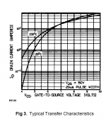
Graf said for what the currents and temperature as UDS.
Yes, the chart says that the transistor, which is a little more heated, do all the work himself and will go immediately into the silicon heaven!
But I would rather wait for practical results.
But I would rather wait for practical results.

 It is the belittling attitude that I have issue with, not the fact that multiple FETs with no source resistors may blow up. You have all made this statement nicely now in language that doesn't offend people or scare them away so I think the point has been made.
There is no need to insult, degrade and humiliate another member just because his/her design is not "as good" as yours. Please, lets make this a civil meeting place befitting our honourable profession.
There is no need to insult, degrade and humiliate another member just because his/her design is not "as good" as yours. Please, lets make this a civil meeting place befitting our honourable profession.
a) You seem to have some issues understanding what's up. It's certainly not about "mine is better" but about something that puts potential innocent/inexperienced DIYers at risk. I'm pretty sure you would not enjoy assuming responsability for hosting an irresponsibly dangerous design. Also, looking at the author position, this certainly does not qualify as a honest mistake, "perseverare diabolicum" applies.
b) I'm sure you meant "honourable hobby" rather than "honourable profession"
I'll skip for the moment any rants about intellectual property and copyright issues related to the incumbent's site (dutyfully promoted by the author with your generous moderation support), at least until you'll have a chance to review your own policies about.
Last edited:
Id limited at 50A (for Ugs=10V) or more you call protection? Or you saw some schematics with old laterals and copyied it to your "invention"?diodes D101 and D102 serve as current protection.
Id limited at 50A (for Ugs=10V) or more you call protection? Or you saw some schematics with old laterals and copyied it to your "invention"?
Transistors so selected to have the same characteristics, only those transistors can be used.
As transistors have the same characteristics, sweeping the input voltage, I reach the current limit.
Please look carefully, you do not have language problems.
TranslateGoogle
Last edited:
I suggest you read this Federmann :
http://www.irf.com/technical-info/appnotes/an-1155.pdf
http://powerelectronics.com/704PET23.pdf
Although being aware of the issue, I had not seen those documents before. Thanks for posting! I like their humor by the way... 🙂
Figure II-3: Visual Image of the IRF1405Z failure. This type of visual
pattern is more attractive when observed on the surface of the moon,
instead of on the surface of parts that are trying to land there.
An externally hosted image should be here but it was not working when we last tested it.
I know that I did not say anything, so your decision is wrong, diodes D101 and D102 serve as current protection.
Have a beautiful night.
Federmann,
just of curiosity can you tell us what is the current through transistors T107 and T108?
And what are the resistor values of R114 and R115?
Thank you!
BTW, does Mr Federmann like Valhalla cables?
Cheers Michael
Last edited:
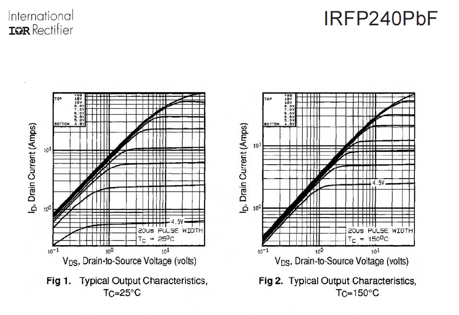
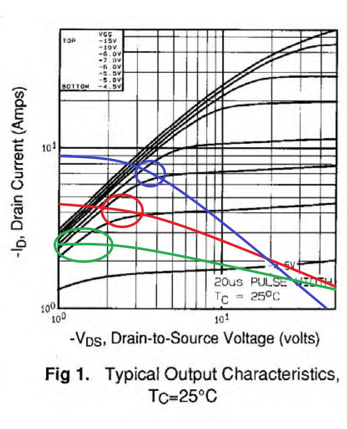
I am looking carefully, Ids for Vgs 10V (limit by Zener diode) and Vds 40V is more than 40A. It is visible in posted graph (second curve from top). This are conditions with shorted output. With Vds 40Vx40A= 1600W to dissipate for one mosfet.. Nice firework.
Last edited:
- Status
- Not open for further replies.
- Home
- Amplifiers
- Solid State
- Topology Federmann, HQQF-55 ...