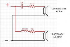
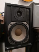
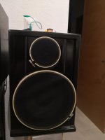
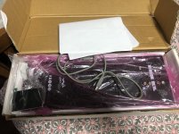
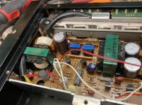
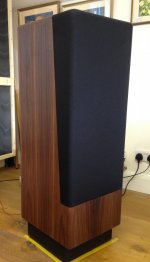
First of all, happy new year everyone! 🎄🎉
Not too long ago I became interested in current drive amplifiers (I'm
not suggesting to discuss pros and cons here!) and also I was looking for a hobby project, so for the sake of curiosity I decided to design a low power current drive headphone amplifier. Normally I don't do electronic design, therefore it took some time to come up with a circuit that satisfies my wishes. It still is a virtual thing and I'd appreciate any feedback from you guys on whether it's a sensible design.
Some goals and restrictions are:
- the amp should drive my ATH-M50X headphones well (which is easy with their 38 Ω flat impedance characteristic and high efficiency of 99 dB SPL at 1 mW [or sensitivity of about 113 dB at 1 V RMS])
- THD under 0.01% or -80 dB
- can use SMT components, but only with pitch of at least 1.27 mm
Please find attached the schematic circuit I came up with, as well as the LTspice project archive.
The two frequency response graphs are for C4 absent and present (input / voltage gain stage bandwidth limiting). Phase near 20 kHz is better without it and its efficiency is doubtful with the gain of 3 or even 1.5 (depending on whether R3A or R3B is used, which are for 1 V RMS sources and 2 V RMS sources correspondingly). I guess, I'll keep a place for it on a PCB (which is not designed yet), but won't put the capacitor initially.
The output impedance graph shows a quite even line at over 145 kΩ over the whole frequency range. I guess, this is very high for an audio amplifier.
THD at full power with 38 Ω load (28 mW) is under 0.02%, which is higher than the goal of 0.01%, but it goes much lower at lower power and there is enough headroom for ATH-M50X (which require only 12.5 mW to reach 110 dB SPL).
A few words about the design.
The input / voltage gain stage is as typical as possible, no comments.
The output stage is the defining part of the amplifier. It consists of two improved Wilson current mirrors (with emitter degeneration resistors) forming a bidirectional current source, which is driven by a class AB bidirectional current sink (with diode biasing) built around U2 and Q1.1–Q2.2. All the transistors are matched pairs of the same type, and U1–U2 can be a single OPA1642 (or with some range checks and adjustments OPA1656 or virtually anything else).
The improved Wilson current mirror has the least distortion of all BJT current mirrors I tried, but the emitter degeneration resistors are still preferred as they lower it even further. The booster after U2 is built in class AB to minimize distortion comparing to a class B booster or a whole op amp powered by the current mirrors.
Are you interested and/or have questions? What do you think about such an amplifier?
2020-01-02 update
Perhaps, it makes sense to clarify the limits of the "low power". The design demonstrates reasonable distortion level (less than 0.05%)
at maximum power (remember, it declines with output power / volume) providing up to about 40 mA (with Rref = 100 Ω) into up to about 70 Ω load (lower impedance load will stress the output stage less, so the distortion will be less).