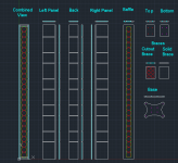
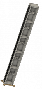
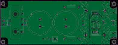
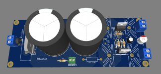
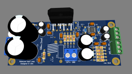
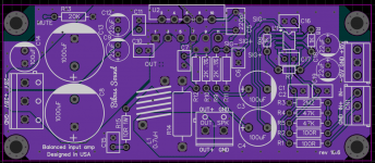
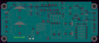
Balanced input LM3886 design and PCB layout
Here is my take on the balanced input LM3886 implementation.
Edited on 6-5-2022 with many small improvements to the schematics.
Edited on 7-16-22.
Edited on 12-23-2022
The gain for the LM3886 was eventually set to 10.
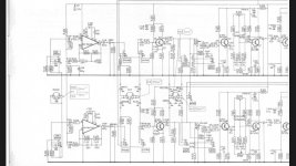
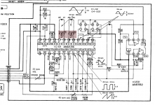
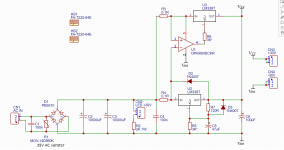
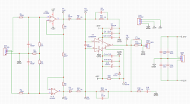
Circuit topology is an instrumentation amplifier. Balanced signal is fed into high-pass filter (100R, 100pF). We then have LM4562 opamp to provide impedance matching to the inputs of the LM3886. LM3886 chip amp is then fed two differential signals to its inverting and noninverting inputs and acts as a difference amplifier.
The gain of the LM3886 is set to 10 and is defined by the relation of the feedback resistor Rf = 20K and the input resistor Ri = 2K. Because we are using the chip amp at its minimum stable gain of 10, the stability network of Cf and Rfs is modified to omit the resistor. Otherwise, the gain of the amp is divided in two at the frequency of Cf and would equal to 5 - potentially a source of instability (in my opinion).
To ensure the HF stability two 27pF capacitors are added.
Resistors R8, R9, R10, and R11 determine CMRR or the whole circuit and should be at least 0.1% tolerance - this will allow for theoretical 66 dB CMRR. Better tolerances will allow for better CMRR, but will be limited by CMRR rating of the LM3886 itself.

Just a side note: 10K resistor has Johnson noise that is -112 dBU (across 20KHz range, at 20 degrees C) - according to this online calculator: https://www.daycounter.com/Calculators/Thermal-Noise-Calculator.phtml.
Feedback resistor Rf and input resistor Ri are both connected to the inverted input of the chip amp. To balance that, we need to mirror the same values for non-inverted input, except we connect resistors to the input and to the ground. This arrangement created what is known as a difference amplifier.
Since both input resistors are 2K we need a buffer to interface to the outside world and to be able to present at least 10K of impedance to connected devices.
Differential input resistance is 2 * 47K = 94K.
Common mode resistance is 47K + 2 * 2.2M = 4.447Meg.
For the balanced inputs the level of the signal is usually 4Vrms per channel. Half of that is 2. After RMS conversion 2 * √2 = 2.8284 Vpk. With the minimum gain of 10, the output voltage chip amp has to be able to handle is therefore 2.8284 Vpk * 10 = 28.284 Vpk. This is possible because LM3886 can be powered +-28V max into 4 ohm loads.
Dissipated power is another factor that determines maximum allowable power output by the LM3886:
Pd = Vcc^2 / 2* Pi^2 *Rload
For 28V supply and 4 ohms load: Pd = 784 / 19.7292 = 39.7380W
For 30V supply and 4 ohms load: Pd = 900 / 19.7292 = 45.6407W
Note that non insulated LM3886 can dissipate 40W without the fan, and insulated LM3886 can only dissipate 30W.
In our case, power supply is +-28V. We also need to subtract up to 5V for 4 ohm loads and 2.7V for 8 ohm due to chip voltage drop. 28V - 5V = 23Vpk of max output voltage swing without the distortion.
In the schematics input buffers are configured with the gain of 1+ 2 * 1K / 20K = 1 + 0.1 = 1.1. The gain of the differential stage is 10. Total gain is 10 * 1.1 = 11.
Edited on 6-5-2022 with many small improvements to the schematics.
Edited on 7-16-22.
Edited on 12-23-2022
The gain for the LM3886 was eventually set to 10.
Circuit topology is an instrumentation amplifier. Balanced signal is fed into high-pass filter (100R, 100pF). We then have LM4562 opamp to provide impedance matching to the inputs of the LM3886. LM3886 chip amp is then fed two differential signals to its inverting and noninverting inputs and acts as a difference amplifier.
The gain of the LM3886 is set to 10 and is defined by the relation of the feedback resistor Rf = 20K and the input resistor Ri = 2K. Because we are using the chip amp at its minimum stable gain of 10, the stability network of Cf and Rfs is modified to omit the resistor. Otherwise, the gain of the amp is divided in two at the frequency of Cf and would equal to 5 - potentially a source of instability (in my opinion).
To ensure the HF stability two 27pF capacitors are added.
Resistors R8, R9, R10, and R11 determine CMRR or the whole circuit and should be at least 0.1% tolerance - this will allow for theoretical 66 dB CMRR. Better tolerances will allow for better CMRR, but will be limited by CMRR rating of the LM3886 itself.
Just a side note: 10K resistor has Johnson noise that is -112 dBU (across 20KHz range, at 20 degrees C) - according to this online calculator: https://www.daycounter.com/Calculators/Thermal-Noise-Calculator.phtml.
Feedback resistor Rf and input resistor Ri are both connected to the inverted input of the chip amp. To balance that, we need to mirror the same values for non-inverted input, except we connect resistors to the input and to the ground. This arrangement created what is known as a difference amplifier.
Since both input resistors are 2K we need a buffer to interface to the outside world and to be able to present at least 10K of impedance to connected devices.
Differential input resistance is 2 * 47K = 94K.
Common mode resistance is 47K + 2 * 2.2M = 4.447Meg.
For the balanced inputs the level of the signal is usually 4Vrms per channel. Half of that is 2. After RMS conversion 2 * √2 = 2.8284 Vpk. With the minimum gain of 10, the output voltage chip amp has to be able to handle is therefore 2.8284 Vpk * 10 = 28.284 Vpk. This is possible because LM3886 can be powered +-28V max into 4 ohm loads.
Dissipated power is another factor that determines maximum allowable power output by the LM3886:
Pd = Vcc^2 / 2* Pi^2 *Rload
For 28V supply and 4 ohms load: Pd = 784 / 19.7292 = 39.7380W
For 30V supply and 4 ohms load: Pd = 900 / 19.7292 = 45.6407W
Note that non insulated LM3886 can dissipate 40W without the fan, and insulated LM3886 can only dissipate 30W.
In our case, power supply is +-28V. We also need to subtract up to 5V for 4 ohm loads and 2.7V for 8 ohm due to chip voltage drop. 28V - 5V = 23Vpk of max output voltage swing without the distortion.
In the schematics input buffers are configured with the gain of 1+ 2 * 1K / 20K = 1 + 0.1 = 1.1. The gain of the differential stage is 10. Total gain is 10 * 1.1 = 11.

![[IMG]](https://live.staticflickr.com/65535/51796862716_35a208e988_c.jpg "[IMG]")
![[IMG]](https://live.staticflickr.com/65535/51796983573_2a87906c2c_c.jpg "[IMG]")
![[IMG]](https://live.staticflickr.com/65535/51795915167_1de2b29de5_o.jpg "[IMG]")
![[IMG]](https://live.staticflickr.com/65535/51795915277_4ae67dc264_c.jpg "[IMG]")