

This is just an area I can blab on about stuff without it using up bandwidth in the threads  Hopefully someone will find it interesting or useful.
Tony.
Hopefully someone will find it interesting or useful. Tony.
Construction of a P2P LM3886 gainclone part 1.
Posted 19th November 2009 at 09:18 AM by wintermute
Updated 17th April 2011 at 01:19 PM by wintermute (Added to category amplifiers)
Updated 17th April 2011 at 01:19 PM by wintermute (Added to category amplifiers)
edit: 17th April 2011. Just to set the record straight, although I refer to this chipamp as a "gainclone" strictly speaking it is not. A gainclone is I believe actually a clone of the 47 labs gaincard, however many people refer to chipamps as gainclones incorrectly (myself included).
edit: apologies to anyone viewing this at less than 1280 screen width... It formats properly with that (two images side by side) but I'm not going to go and redo all the images now!!! I already did twice....
Well I said about 4 years ago that I would do a build writeup for my P2P gainclone. I took all of the pictures but never got around to it. I'm off sick and lacking energy so decided it was as good a time as any to have a crack at it
I started out with the BrianGT schematic. I wanted to build something that people were using and was likely to just work. Here is a copy of the schematic

Note I did not use a volume pot or the mute switch) but all other components are as per the schematic (including optional ones).
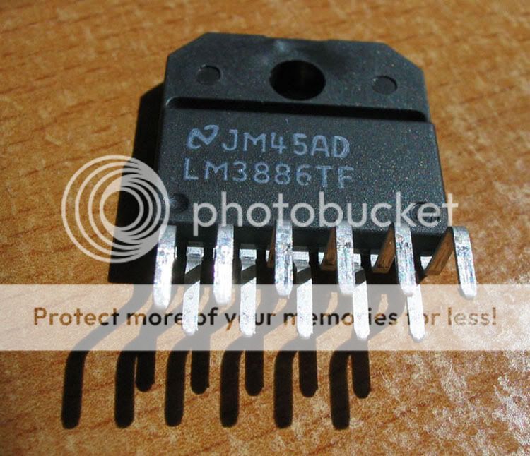
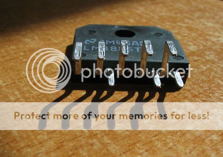
First off some pictures of the chip itself.
1. 2.
2. 
3.
1. The chip before any modifications. 2. The chip after carefully clipping off the legs that were not needed. The carefully bit was making sure I was chopping off the right ones!!!! 3. attaching a link for the +ve power so I only had to run one +ve lead, a piece of enameled copper wire did the trick.
Because of the closeness of the pins on the chip I decided it was easiest to build up "modules" and then attach them to the chip. First module was the + and - local decoupling caps. These are 100uF 50V Nichicon FG caps bypassed by Wima 0.1uf Polyester caps (I chose to use polyester for size reasons).
4. 5.
5. 
4. I bent the leads to make it easy to solder, just slide them over and then solder in place as per 5.
6. 7.
7. 
6. simply shows the bending over and soldering of the Zero Volts side of the Decoupling caps. This forms one of the three earth returns to the star point on the PS board. 7 shows the addition of the mute resistor.
8. 9.
9. 
8. Shows the addition of the Mute capacitor, and 9. shows the bending of the leads such that they should slide over the pins of the LM3886 to make it easy to solder on. By using the legs of the capacitors as the connection to the pins on the LM3886 it certainly meets the requirement in the datasheet that the decoupling caps should be as close to the chip pins as possible
10. 11.
11. 
Next I decided to tackle the feedback parts of the circuit. 10. shows the 1st (22k) feedback resistor soldered to the chip, and the feedback capacitor with the second (680r) resistor soldered to the cap sitting beside it. 11. shows the cap + resistor soldered to the chip.
12. 13.
13. 
12. shows the earth return for Pin 7 of the chip and the feedback network soldered on. As well as the addition of the 1K and 22K resistors on the input. 13. shows the Decoupling caps module connected to the chip. 14. is another view of the connection of the coupling caps to the chip.
14. 15.
15. 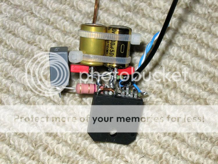
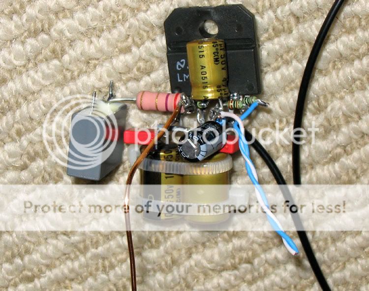
15. shows the addition of the zobel resistor and capacitor to the chip, as well as the input signal wires, which is a very short length of cat5e twisted pair wiring.
16. 17.
17. 
16. is just the view of the chip with zobel resistor and capacitor added from the other side. 17. shows the power supply wiring ready to be soldered on. I braided the wires as I had read that some people think it makes a difference, I have no opinion on that but thought it looked nice.
Well I just went to put the next couple of images in and I had hit the limit, so this is now going to be a multipart Blog entry. Which is ok because at the point I have got up to everything except the power supply connection has been completed. Part two will contain the info on the power supply and final wiring, and maybe even the chassis.
Tony.
edit: apologies to anyone viewing this at less than 1280 screen width... It formats properly with that (two images side by side) but I'm not going to go and redo all the images now!!! I already did twice....
Well I said about 4 years ago that I would do a build writeup for my P2P gainclone. I took all of the pictures but never got around to it. I'm off sick and lacking energy so decided it was as good a time as any to have a crack at it
I started out with the BrianGT schematic. I wanted to build something that people were using and was likely to just work. Here is a copy of the schematic
Note I did not use a volume pot or the mute switch) but all other components are as per the schematic (including optional ones).
First off some pictures of the chip itself.
1.
2. 3.
1. The chip before any modifications. 2. The chip after carefully clipping off the legs that were not needed. The carefully bit was making sure I was chopping off the right ones!!!! 3. attaching a link for the +ve power so I only had to run one +ve lead, a piece of enameled copper wire did the trick.
Because of the closeness of the pins on the chip I decided it was easiest to build up "modules" and then attach them to the chip. First module was the + and - local decoupling caps. These are 100uF 50V Nichicon FG caps bypassed by Wima 0.1uf Polyester caps (I chose to use polyester for size reasons).
4.
5. 4. I bent the leads to make it easy to solder, just slide them over and then solder in place as per 5.
6.
7. 6. simply shows the bending over and soldering of the Zero Volts side of the Decoupling caps. This forms one of the three earth returns to the star point on the PS board. 7 shows the addition of the mute resistor.
8.
9. 8. Shows the addition of the Mute capacitor, and 9. shows the bending of the leads such that they should slide over the pins of the LM3886 to make it easy to solder on. By using the legs of the capacitors as the connection to the pins on the LM3886 it certainly meets the requirement in the datasheet that the decoupling caps should be as close to the chip pins as possible
10.
11. Next I decided to tackle the feedback parts of the circuit. 10. shows the 1st (22k) feedback resistor soldered to the chip, and the feedback capacitor with the second (680r) resistor soldered to the cap sitting beside it. 11. shows the cap + resistor soldered to the chip.
12.
13. 12. shows the earth return for Pin 7 of the chip and the feedback network soldered on. As well as the addition of the 1K and 22K resistors on the input. 13. shows the Decoupling caps module connected to the chip. 14. is another view of the connection of the coupling caps to the chip.
14.
15. 15. shows the addition of the zobel resistor and capacitor to the chip, as well as the input signal wires, which is a very short length of cat5e twisted pair wiring.
16.
17. 16. is just the view of the chip with zobel resistor and capacitor added from the other side. 17. shows the power supply wiring ready to be soldered on. I braided the wires as I had read that some people think it makes a difference, I have no opinion on that but thought it looked nice.
Well I just went to put the next couple of images in and I had hit the limit, so this is now going to be a multipart Blog entry. Which is ok because at the point I have got up to everything except the power supply connection has been completed. Part two will contain the info on the power supply and final wiring, and maybe even the chassis.
Tony.
Total Comments 6
Comments
-

LM3886 amplifier
looks good tony - how is progress going with the amplifier?Posted 6th August 2010 at 01:02 AM by nuryev

-
 Hi nuryev It's been finished for quite a while about 5 years in fact! But ironically I've only really been using it for main amplifier duty for a short while (after problems with my main amp). It performs very well to my perhaps not so golden ears. Seems perfectly happy driving my rather low impedance (around 3 ohms at their worst) speakers too.
I made the blog entries a long time after the construction mainly so it was documented and so some others might get some value from it.
Thanks for the comment! Pt II has the rest of the details
Tony.Posted 6th August 2010 at 08:34 AM by wintermute
-
 Wow! Good P2PPosted 3rd July 2011 at 06:48 PM by availlyrics
-
Thanks!
Tony.Posted 4th July 2011 at 01:09 PM by wintermute
-
Obviously you adopted the P2P philosophy to reduce consumption of wire. In the amp there is about 10mm of wire, all the rest are the very shortened component leads.
There must be some Aberdonian in you !
Or do you know something about the price of copper?
Nice work.Posted 31st May 2014 at 07:09 PM by AndrewT
-
I missed this comment Andrew! Thanks it gave me a chuckle I'm not sure exactly what possesed me to make it so compact, probably just because I could!!
I regret it a bit now as I would have liked to have tried it with a lower gain, but it is too difficult to do once it is built.
It is still in service now as the mid/tweeter amp in my bi-amped setup with 10" woofers running off my playmaster series 200. One day I will get around to building my BA3 complementary which will take over from this and it will then be my speaker testing amp once again.
Tony.Posted 26th April 2017 at 01:44 PM by wintermute

