And here are some pictures about it.
>The IR MOSFETs (big Qgd) and Gate Drivers are really so slow. The Vishay, Fairchild, and SGS Thomson MOSFETs are much better, as John wrote.
>I think the switching speed have not to be risen. I think that the ideal fsw is about 300-400 kHz. The distorsion can be reduced with feedback. All of the amplifier giants (Crown, Powersoft) applies analog output stage of its interest. And with analog output, the class I topology can be made easily without dead time! The feedback also reduces the phase shift to 1 degree at 100 kHz in-to-out signal in Crown's circuits. This can also be made with a fast DSP with all of the input signal decoding, etc..
Attachments
Hi Gyula,
good to see somebody else from Hungary in this forum...
I think a D/A in the feedback isn't a good idea becouse of the propagation delay of the D/As...
Try a bare analogue FB or a bare Digital or mixed...
Hi anybody,
I agree with posts about No FB amps switching ferquency and jitter/ supply modulation caused output distortions...
I know that the lower the PWM ferqu, the smaller is (relative) the jitter and switching caused distortion...
However this also means that the less jitter and higher quality (speed) power stage I have the better the output is with respect to distortion. At the same time the higher the PWM frequ is, the greater the AMPs power bandwith will be (and the less the open loop output impedance)...
I just tought that a bare DSD signal driven amp could (maybe)sound good... ( and I think the SHARP uses an 5.6Mhz PWM and sounds good)
On the other hand I agree that a 768kHz digital modulator is enough in speed and is a good compromise between bandwith and efficiency and distortion.
However NFB certainly lowers the distortions and the output impedance, an overall FB is not allways good becouse of the low speed of the circuit. Generaly I think even if I use NFB I must have a design wich have very small distortion and output impedance even in open loop... (and in analogue circuits I use small loops instead of one big overall FB)...
Does anybody know some technique for operating the TAS 5015 @768kHz?
Thanks,
Tako Tamas
The Sharp is based on PDM modulation @ 64Fs as DSD, you could build one around the CS4303 which provides 64Fs outputs.
TT, I don’t agree that increasing the switching rate reduces the output impedance – the output impedance of an open-loop Class D amp is determined by the PSU impedance & MOSFET RdsOn. How does increasing the Switching rate reduce these variables?
If anything, the impendence of a output stage operated at higher switching frequencies will be worst, due to the greater occurrences of undefended states on the switching edges – where the output is nether truly High or Low.
The helping hand of feedback should be treated as a friend, and should never be taken advantage off. Its always sound engineering to make a system as linear as possible before the application of feedback.
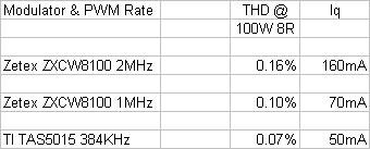
Below is a small table of the same Open-Loop output stage operated from 384KHz to 2MHz into 100W 8Ohms with comparisons of THD & quiescent current due the higher PWM Fs, as can be seen the THD performance worsens at higher PWM Fs: -
TT, I don’t agree that increasing the switching rate reduces the output impedance – the output impedance of an open-loop Class D amp is determined by the PSU impedance & MOSFET RdsOn. How does increasing the Switching rate reduce these variables?
If anything, the impendence of a output stage operated at higher switching frequencies will be worst, due to the greater occurrences of undefended states on the switching edges – where the output is nether truly High or Low.
The helping hand of feedback should be treated as a friend, and should never be taken advantage off. Its always sound engineering to make a system as linear as possible before the application of feedback.
Below is a small table of the same Open-Loop output stage operated from 384KHz to 2MHz into 100W 8Ohms with comparisons of THD & quiescent current due the higher PWM Fs, as can be seen the THD performance worsens at higher PWM Fs: -
Attachments
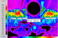
Below is a thermal image of the output stage in the above post. The emittance of the IR Imager has been set to 0.9% to allow correction for the MOSFET package “IR Transparency”, from previous work I’ve calculated that this gives a accurate idea of DIE temperature, and not just the package surface. The output stage design uses 2x Pch and 1x Nch MOSFET’s per H-Bridge side to equalise their RDS-on values.
In fact, it can be observed that the centre Nch devices are hotter than the outer Pch devices on each arm of the H-Bridge (The Black (cold) Circle between each arm of the H-Bridge - in the centre of the PCB is the Bulk PSU reservoir capacitor).
Note: - in the right hand side of the image, the Text label for the Nch FET has been overlayed by the Pch label - but its the hotter device in the middle.
It’s common to see this effect at idle (no signal), due the normally slower switching P-Ch devices causing higher Shoot-thru current in their Nch Counterpart. However, at higher power levels RdsOn losses becomes the dominant heating factor.
As can be seen from the thermal image of the PCB below - at 1KHz 111W 8Ohms (PWM Rate 384KHz) for 20 minutes, the worst case FET die temperature is around 46Deg. the thermal results are without any form of heat sinking – apart from the 2-ounce copper PCB – try doing this with Class B!!!
Attachments
Hi JohnW and TT,
at least one other thing influences the output impedance: the output filter. Therefore this is one of the most important parts, especially in open loop designs. But a higher switching frequency allows the filter's L, R and C values to be reduced and the upper signal frequency will raise to an appropriate value. So the filter-induced distortions should be lowered as well as output impedance.
And, if a hard switching power stage is to be used, it should switch even well defined, with rise and fall times going down, corresponding to increased frequency. Yes, yes, yes, I know the problems with ringing and spikes and phantom switching... They still occur also on my "PCB".
The table is interesting: without or with the same output filter?
In fact I agree with the statement of JohnW: using a NFB simplifies the matter. If not that, what is the reason for Philips, Mueta and some others to praise their (multiple feedback-) designs as nearly distortion-free? I've also never heard any of them (if I only could...), but particularly Muetas measuring sheets look very impressive.
http://www.mueta.com/App_sheet_DL.pdf
http://www.mueta.com/Whitepaper.pdf
http://www.mueta.com/AES.pdf
Regards, tiki
Hi JohnW,
That is right. The RDSon and the Supply impedance are very important. (except if bipolar is used... )
)
BUT: those amps uses an output filter with one or two serial inductance (typical a few uH). This means without feedback an increasing "resistance". If I use a higher PWM frequ, I can use smaller "L" wich is smaller "resistance". This can be also a point at higher frequencies like F>1kHz of audio output.
So the PWM frequ is a further point in output impedance.
Thanks,
TT
That is right. The RDSon and the Supply impedance are very important. (except if bipolar is used...
)BUT: those amps uses an output filter with one or two serial inductance (typical a few uH). This means without feedback an increasing "resistance". If I use a higher PWM frequ, I can use smaller "L" wich is smaller "resistance". This can be also a point at higher frequencies like F>1kHz of audio output.
So the PWM frequ is a further point in output impedance.
Thanks,
TT
Hi TT,
Once again, I don’t understand how using a Bipolar removes the PSU impedance issues, nor for that matter RdsOn - or in the case of a Bipolar its effective emitter resistance. Bipolar are very poor saturation-switchers, and only FB can correct for the above limitations.
Your quite correct in stating that a higher PWM Fs rate allows a higher LPF corner frequency, but you would have to have very poor quality inductors before there DC resistance approached anything like the combined “resistance” of the PSU / RdsOn as seen by the load.
If you take a closer look at my PWM Fs comparison table, there’s a more then doubling in THD, from 384KHz to 2MHz – this is with the best OPS I can design. This increase has nothing to do with the inductor - reducing its value or even removing completely is not going to help.
What about the effect of increasing output impedance due to the greater amount of edge transitions - this effect will swamp any benefit gained by reducing the copper losses of the smaller value inductor(s).
There is one very definite advantage to reducing the value of the inductor (rising the corner frequency) – and that’s to reduce the sensitivity of the class D output LPF response to output load variations.
It’s very normal to see a sharp increase in input impedance of a typical box loud speaker at HF. This increase causes a very sharp PEAK in the frequency response of a digital amplifier. The fix for this is to have a Zobel network in the Speakers Crossover - to synthesize a “constant” impedance at HF. Unfortunately; this is in direct conflict with the requirements of Class AB amps, which perform better into high impedance loads - as this reduces there Class AB output stage crossover distortion.
I use ESL's, which have the opposite problem, but a gentle HF roll-off is much preferred to a sharp peak!
If users find there digital amplifiers sounding “bright” or “sibilant” – I recommend trying a simple RC Zobel network across there speakers. A simple sound level pressure meter & a spot-tone test CD should help find the correct values.
Hi Tiki,
The output stage is identical in all respects, only the modulators have been changed (on Plug-in cards).
The DC losses of a well designed inductor are small compaired to PSU & RDS-on issues.
I find that the inductor performance (Amidon Type 2 cores) only becomes an issue once the other OPS distortions have been reduced to below 0.002%
Regards,
John
The higher the switching frequency, linearly lower the inductance of the integrator, at the same peak inductance currents. This is true. And, the lower the inductance, the lower the output phase shift. But, the output level is always will be determined by the duty factor and the voltage loss of the ohmic resistances before the outputs.
The lower the inductance of LC integrator, the higher the dv/dt capability (lower phase shift, related to sinusoidal wave) of the output at rated load. The filter dimensioned far above the high pass frequency of the modulator in order to reject the square-wave switching signal from the outputs. So the higher dv/dt capability is only needed when you don't use feedback, because of the phase shift (I think), and maybe because of the "damping factor" when the inductive loudspeaker gives the magnetic field back to the amplifier. Then the little inductance is necessary by the inductive voltage division. (This is why the Crown's class-I is better than class-D)
Back to a story about the output inductances: I made my first circuit two years ago. At that time I don't care about the filter components so much. There was two 2-way crossover getting dusty in my clutter boxes, I was searching for an inductor (the capacitor have been decided before to be 1 micro Farad ) and think: 'These will be ideal !'. The circuit was based on a flash ADC and two 8-bits binary counters, and worked at 125 kHz. The results were amazing. At low volume the sound were terrible, noisy and detailless, but increasing the volume it was improved rapidly, and at max. volume the sound were clear, crispy and dynamic, much better than the Quad-405 sounds. Later turned out that the coil is 220 micro Henry.
That circuit was much more better with the 125 kHz 8-bit modulation and 220 micro Henry, 1 micro Farad LC filter than the other, which has optical digital input, TAS5012 drived (384 kHz) 12 micro Henry 750 micro Farad LC filter at 96V; the measured signals are better, the sound is worse.
The output phase shift, dead-time, and non-resistive errors can be reduced to acceptable level only with feedback (I think). But the calculate of feedback is very complex. And as ttako wrote, there's a delay in digital systems. But there is also in analog modulators because of the triangle wave (and the modulation itself)
The digital system has added delays because of the error calculation, modulation algorythm, and maybe of the interpolation (depends on where the signal feeded back).
The file contains the 125 kHz 8-bits digital amplifier schematics in CorelFlow 2.0 format.
Good luck for everybody!
The lower the inductance of LC integrator, the higher the dv/dt capability (lower phase shift, related to sinusoidal wave) of the output at rated load. The filter dimensioned far above the high pass frequency of the modulator in order to reject the square-wave switching signal from the outputs. So the higher dv/dt capability is only needed when you don't use feedback, because of the phase shift (I think), and maybe because of the "damping factor" when the inductive loudspeaker gives the magnetic field back to the amplifier. Then the little inductance is necessary by the inductive voltage division. (This is why the Crown's class-I is better than class-D)
Back to a story about the output inductances: I made my first circuit two years ago. At that time I don't care about the filter components so much. There was two 2-way crossover getting dusty in my clutter boxes, I was searching for an inductor (the capacitor have been decided before to be 1 micro Farad
) and think: 'These will be ideal !'. The circuit was based on a flash ADC and two 8-bits binary counters, and worked at 125 kHz. The results were amazing. At low volume the sound were terrible, noisy and detailless, but increasing the volume it was improved rapidly, and at max. volume the sound were clear, crispy and dynamic, much better than the Quad-405 sounds. Later turned out that the coil is 220 micro Henry.That circuit was much more better with the 125 kHz 8-bit modulation and 220 micro Henry, 1 micro Farad LC filter than the other, which has optical digital input, TAS5012 drived (384 kHz) 12 micro Henry 750 micro Farad LC filter at 96V; the measured signals are better, the sound is worse.
The output phase shift, dead-time, and non-resistive errors can be reduced to acceptable level only with feedback (I think). But the calculate of feedback is very complex. And as ttako wrote, there's a delay in digital systems. But there is also in analog modulators because of the triangle wave (and the modulation itself)
The digital system has added delays because of the error calculation, modulation algorythm, and maybe of the interpolation (depends on where the signal feeded back).
The file contains the 125 kHz 8-bits digital amplifier schematics in CorelFlow 2.0 format.
Good luck for everybody!
Attachments
I think, the problem is not the "output filter error" (maybe the phase shift, Fourier-line calculations), but the dead-time caused flattening, what is rising if the switching freq. is increased. The higher the frequency, the larger the error you get. This will never can be discounted with feedbackless class-D designs.
Tiki, the ringing maybe get reduced with schottky clampers, or with slowering down the dv/dt of output transistors. I think the zero error hard-switching output isn't realizable. High voltage (above 200V) output stages can be made with Warp IGBTs from IRF, or SMPS II series from Fairchild. But because of the tail currents caused long deadtimes, there must be a feedback from outputs.
The amplifiers are being made by Crown, etc... uses analog modulation with feedback. The I-Tech from Crown is the best I have ever seen, 8000W RMS at near audiophile quality.
Thank you for your hints!
If you are interested, look at http://www.ibtk.de/project/class_d/pictures/classd_011_1280x960.jpg and you may see the reason for my problems, I'm a beginner in ClassD.
http://www.ibtk.de/project/class_d/pictures/dscn3198_1k.jpg shows the ringing after inserting freewheeling FREDs and Schottkies. In the next design I want to try out Infineons SIC-Schottkies, because of virtual zero recovery current. Has anyone experiences with them?
http://www.ibtk.de/project/class_d/pspice/ver_0.3/20040202_classd-generator_03_schematic.pdf is a simulation schematic of the current N/P-output stage. The gate driver is still ICL7667, the FETs are IRFU5305 and RFD14N05.
May be, it is a problem of poor decoupling of the supplies (1000uF+100nF X7R) or too long gate wiring in combination with the C=330n at the driver and the Cs of the Gate and the protection diodes (P6KE15). I hope to solve some of it with a dedicated PCB.
Is there a suggestion for the pure N-stage FETs, I would start with FQP34N20 (200V, 60nC), driven by MIC4420?
I found out, that the "optimum" deadtime for this design is about 200ns at 700kHz, giving the lowest quiescent current and nearly no audible noise through the speaker. This seems to be very long, but shorter deadtimes result in heavy ringing at the gates and therefore massive shoot-through.
Regards, Timo
Hi,
John, thank you for putting this thread into right tracks again. I got a little tired defending 5MHz switching .
Tiki, I have tried SiC Schottky in 3kW PFC boost converter. It was not Infineon, but from CREE corporation. It had replaced IR Hexfred diode. I did not look at the waveform, since at 400V switching overshot is almost nonexistent, but I checked conducted EMI interference and it improved considerably. Also efficiency has improved, so I can wholeheartedly recommend them. You might only have problems with relatively high forward drop. I intend to use them in multiphase BCA power stage that will complement my multiphase modulator.
200ns dead time might be good for amplifiers with feedback, but for open loop designs it is too much. Here are some of my experiences:
Good decoupling is a must. Contrary to the expectation, it is advantageous to have not only C but RC series connection across each switching pair. I have not yet tried local decoupling with small series L that TI is proposing in all their output stages. More info is in this patents: patent1 patent 2
Did you take a look at the Spectron patent I posted? This output stage is actually used in Spectron 500W output stages.
Another weird thing I have discovered is that it is better to drive gates with cca 400nH inductor instead of a resistor. Gate waveforms are free of oscillations Of course you must decouple inductor with schottky diodes to gnd and supply voltage at both ends of the inductor.
I have also tried complementary mosfets, but in source follower orientation. Advantage is that you can not have both fets on at the same time, no mater how fast your gate circuit is. But then you need floating gate power supply and transformer coupled gate driver. With IRF9530 and IRF530 I have achieved 10ns transition times and cca 10V 10ns spike at the end of the transition. Spike was the same regardless of the supply voltage.
I would also suggest that you try with full bridge output stage,so you can continue to use 100V fets and you will also not have problems with power supply pumping at low frequencies.
Another way to achieve clean switching is by use of zero voltage switching technique. In this case you need very small filter inductor since peak ripple current must be larger than your output current. Advantage is that you can use extremely large mosfets, since switching is lossless. Disadvantage is that you get asymmetric transition times with load and more elaborate driver circuit. I think this is proper way for amplifiers with feedback. Take a look at this APT application note .
I have no recent experience with modern low power mosfets (I only do medium and high power at the moment). I know Tripath recommends ST, and I found that currently Fairchild have the best figure of merit (gate charge x Rdson). I would like to ask how is with the ruggedness of current small power mosfets? 10 years ago Siliconix and ST would fail within seconds in the same circuit where IRF and Motorola could take any abuse thrown at them. Have the thing changed?
Last, for those interested in state of the art fast switching, here is the link to the Directed Energy website. Read application notes.
Best regards,
Jaka Racman
John, thank you for putting this thread into right tracks again. I got a little tired defending 5MHz switching
.Tiki, I have tried SiC Schottky in 3kW PFC boost converter. It was not Infineon, but from CREE corporation. It had replaced IR Hexfred diode. I did not look at the waveform, since at 400V switching overshot is almost nonexistent, but I checked conducted EMI interference and it improved considerably. Also efficiency has improved, so I can wholeheartedly recommend them. You might only have problems with relatively high forward drop. I intend to use them in multiphase BCA power stage that will complement my multiphase modulator.
200ns dead time might be good for amplifiers with feedback, but for open loop designs it is too much. Here are some of my experiences:
Good decoupling is a must. Contrary to the expectation, it is advantageous to have not only C but RC series connection across each switching pair. I have not yet tried local decoupling with small series L that TI is proposing in all their output stages. More info is in this patents: patent1 patent 2
Did you take a look at the Spectron patent I posted? This output stage is actually used in Spectron 500W output stages.
Another weird thing I have discovered is that it is better to drive gates with cca 400nH inductor instead of a resistor. Gate waveforms are free of oscillations Of course you must decouple inductor with schottky diodes to gnd and supply voltage at both ends of the inductor.
I have also tried complementary mosfets, but in source follower orientation. Advantage is that you can not have both fets on at the same time, no mater how fast your gate circuit is. But then you need floating gate power supply and transformer coupled gate driver. With IRF9530 and IRF530 I have achieved 10ns transition times and cca 10V 10ns spike at the end of the transition. Spike was the same regardless of the supply voltage.
I would also suggest that you try with full bridge output stage,so you can continue to use 100V fets and you will also not have problems with power supply pumping at low frequencies.
Another way to achieve clean switching is by use of zero voltage switching technique. In this case you need very small filter inductor since peak ripple current must be larger than your output current. Advantage is that you can use extremely large mosfets, since switching is lossless. Disadvantage is that you get asymmetric transition times with load and more elaborate driver circuit. I think this is proper way for amplifiers with feedback. Take a look at this APT application note .
I have no recent experience with modern low power mosfets (I only do medium and high power at the moment). I know Tripath recommends ST, and I found that currently Fairchild have the best figure of merit (gate charge x Rdson). I would like to ask how is with the ruggedness of current small power mosfets? 10 years ago Siliconix and ST would fail within seconds in the same circuit where IRF and Motorola could take any abuse thrown at them. Have the thing changed?
Last, for those interested in state of the art fast switching, here is the link to the Directed Energy website. Read application notes.
Best regards,
Jaka Racman
Hi tiki!
I have examined the schematics shown under http://www.ibtk.de/project/class_d/...3_schematic.pdf.
If you would keep capacitive decoupling and the fsw at 700 kHz, I think the following things can help to you:
- The ICL7667 Gate driver has too big output resistance, the peak output current capability is low. Try Microchip TC4421 on heatsinks.
- R84, R85 -> 330 Ohm
- D22, D23 -> 100V 1A Schottky (MBR1100)
- D31, D33 -> 100V 3A Schottky (MBR3100)
- P ch. MOSFET -> 100V 30A
- N ch. MOSFET -> 100V 30A (IRF540N or 2*IRF540 (SGS Th.))
- The MOSFETs should be connected to heatsinks.
- R107, R103, C33, C34, D27, D28 are unnecessary
- D29, D30 have to big trr, this really can cause ringing with fast di/dt. Try 100V 20A Schottkies (MBR20100). The average schottky current is approximately the 1/3 of output current.
- C31, C32 -> 150 nF 50V
- The Power Supply voltage have to be limited to 80V max.
- Power supply set up speed should be reduced to 1V/ms to avoid instant smashing of MOSFETs.
- The PS cables should be twisted to reduce their inductance.
But I think, the overshoots came from the mutual conduction of MOSFETs. If I were you, I wouldn't use capacitive decoupling. I wondered if your 50V FETs don't haven been sizzled at 100V.
Good Luck!
Gyula
Hi Jaka!
I have seen you are planning to make Class-I output stage. I think it's difficult to avoid saturation or exhaustion of the output inductors. The ideal case would be that the inductors are just being exhausted at the beginning of the next charging (polarity swapping). How would you solve this problem?
I have tried a Class-I output with the TAS5012 positive and negative modulated outputs, but the result was wastrel (really). The volume changed in undeterminable way, the circuit sounds like drowing. The coils have been exhausted before their charging cycles. I think the Class-I is easy only with analog modulation because of the symmetry, and adjustable repose duty factor.
Hi Jaka,
Thanks for the Link to the Directed Energy website, some interesting info.
You’re quite right in saying that the ruggedness of current small power MOSFET’s is not in the same league as IR – But I find IR are so slooooow. I use Vishay parts and switch with about 1.2nS hard dead time – as you can see from the thermal image in my earlier post - heating due to cross-conduction is not an issue.
I think your also right in saying Harris have the best figure of merit, but when I last looked, they didn’t have matching Pch’s.
After many very complicated driver circuits with transformers and floating supplies, I gave up on all Nch Bridges – its so much easier just to Cap couple Pch’s. Lower phase noise, faster propagation times, simpler driver stage, which at the end of the day, work out cheaper at the 100W power level.
Does anybody know of any good, fast (matched switching times), cheap, low phase noise all Nch driver circuits? Integrated devices like the Harris HIP2100 (one of the best High / Low side driver) have large and unmatched propagation delays (at least in the sub nS range) and VERY poor Phase Noise, resulting in high open loop distortion.
Compl. stage
Hi John,
The P-channel MOSFETs are less in performance with higher gate charges. The number of P channel FETs must be doubled, the gate charge is quadrupled. The P-ch. and N-ch. FET's turn-on delay time must be different. This causes different duty cicle at the output, which means error voltage on the output.
But the capacitive decoupling is really simplier.
Two story about the ruggedness of IR devices:
First time I misunderstood the inner construction of IR MOSFETs, and designed the output of the early attached "digitalis" circuit without free-wheeling diodes, I thought there is an anti-paralleled schottky diode between the Drain and Source terminals in the MOSFET. The simbols differs from country to country... I have made the first measurements with this clamper-free circuit. --> .zip file
On the picture, the fsw=384 kHz, the square wave sensitivity is 10 V/division, and the sinusoid's (output signal) sensitivity is 1 V/division. There can be seen the shoot througs on the square wave's edges, and they are only about 3,5 V with the MOSFET's body diode! (See the dv/dt of the picture with these body diodes.. what di/dt might belong to it ?)
And the amplifier worked. It was a little bit noisy .
Four things were different from exceptions:
1. The extra noise 2. approximately the double of dissipation
3. Self turn-off at 60% input drive at 4 Ohm load (Here the Vdd is already 96V).
4. The output signal were audible on radio, on the FM band at any frequencies more than 10 metres.
I can't solve the problem for 3 months (I was alone, and really blinded from the light), just searched again and again the noise at the inner digital and analog power supplies (for example: in my fit of despair I fed the analog PLLs from a 4,5V, 3,3V regulated C-Zn battery ). And the effect weren't changed. One day I red a technical paper from IR, about the HEXFET' inner structure  . I have corrected the problem rapidly, and BANG! The earth was moving. The police have been called at my friend, but there was an open-air disco in our village at that time Our loudspeakers were two 120 * 66 * 60 cm reflex cone (called Rutse in my country, 70 kg/piece) with JBL licensed Ukranian loudspeaker.
So, the MOSFETs worked after the correction like they had been in brand new condition.
The cause of the fault was that the spikes reached the output of the TAS, and that switched the Valid outputs to low state.
--
There was an another issue with the IR MOSFETs in the same circuit. Originally I haven't designed Gate discharging resistors for the FETs. One day I had taken out one of the dual Gate drivers from its socket, and accidentally touched the Gate of the FETs, then switched up the power supply (96V 160A peak, 50A continous current capable dumper --> .zip file for schematics). That time the things gone to unexpeced way: The strip connecting the high and low side MOSFETs was disappeared, the Gate drivers was being burnt. One of the Gate driver' left side disappeared with the socket's left side . The TAS was burst at the output side. Under the rebuilding I measured the MOSFETs and usually one of the paralleled devices seemed to be GOOD !!!
First time I misunderstood the inner construction of IR MOSFETs, and designed the output of the early attached "digitalis" circuit without free-wheeling diodes, I thought there is an anti-paralleled schottky diode between the Drain and Source terminals in the MOSFET. The simbols differs from country to country... I have made the first measurements with this clamper-free circuit. --> .zip file
On the picture, the fsw=384 kHz, the square wave sensitivity is 10 V/division, and the sinusoid's (output signal) sensitivity is 1 V/division. There can be seen the shoot througs on the square wave's edges, and they are only about 3,5 V with the MOSFET's body diode! (See the dv/dt of the picture with these body diodes.. what di/dt might belong to it ?)
And the amplifier worked. It was a little bit noisy
.Four things were different from exceptions:
1. The extra noise 2. approximately the double of dissipation
3. Self turn-off at 60% input drive at 4 Ohm load (Here the Vdd is already 96V).
4. The output signal were audible on radio, on the FM band at any frequencies more than 10 metres.
I can't solve the problem for 3 months (I was alone, and really blinded from the light), just searched again and again the noise at the inner digital and analog power supplies (for example: in my fit of despair I fed the analog PLLs from a 4,5V, 3,3V regulated C-Zn battery
). And the effect weren't changed. One day I red a technical paper from IR, about the HEXFET' inner structure . I have corrected the problem rapidly, and BANG! The earth was moving. The police have been called at my friend, but there was an open-air disco in our village at that time Our loudspeakers were two 120 * 66 * 60 cm reflex cone (called Rutse in my country, 70 kg/piece) with JBL licensed Ukranian loudspeaker.So, the MOSFETs worked after the correction like they had been in brand new condition.
The cause of the fault was that the spikes reached the output of the TAS, and that switched the Valid outputs to low state.
--
There was an another issue with the IR MOSFETs in the same circuit. Originally I haven't designed Gate discharging resistors for the FETs. One day I had taken out one of the dual Gate drivers from its socket, and accidentally touched the Gate of the FETs, then switched up the power supply (96V 160A peak, 50A continous current capable dumper --> .zip file for schematics). That time the things gone to unexpeced way: The strip connecting the high and low side MOSFETs was disappeared, the Gate drivers was being burnt. One of the Gate driver' left side disappeared with the socket's left side
. The TAS was burst at the output side. Under the rebuilding I measured the MOSFETs and usually one of the paralleled devices seemed to be GOOD !!!Attachments
- Status
- This old topic is closed. If you want to reopen this topic, contact a moderator using the "Report Post" button.
- Home
- Amplifiers
- Class D
- Anyone interested in a digital amplifier project?