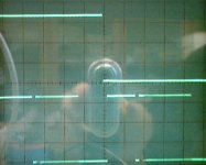
The noise of the output signal is from the analog input of soundcard (Terratec DMX), which have been connected to a signal generator. The oscillogram from the inner I2S bus's data shows the lower bits' continoius changing, this is the noise. The picture shows the CS8416's outputs, the upper signal is the LRCLK out, and the lower signal is the SDATA out.
The output coils have been replaced to Arnold MPP toroids. That's discouted the magnetic coupling of the inductors. The dissipation was also being reduced by this replace.
The output coils have been replaced to Arnold MPP toroids. That's discouted the magnetic coupling of the inductors. The dissipation was also being reduced by this replace.
Attachments
Thank you, especially to John, Jaca and Gyula, for your help!
A last explanation to the simulation circcuit:
- driver ICL has to be replaced by MIC4420 or-21 or Johns suggestion HIP2100 at lower Cgs,
- gate discharge-R: 330Ohm needed? adds approx. 0.3W at Vgs=10V (2 FETs at half time) quiescent power,
- D22, D23 are blocking diodes against too high (and reverse) gate voltage, should have a suppressor behaviour
- D31, D33 have to withstand only gate voltage, 25V should be enough,
- D27, D28 switch off the parasitic body BJT of the MOSFETs, like to be seen in the earlier patent-hint US6304137, several other R/C are for simulator stability only,
- power supply was tried only up to +-25Vmax.
All other hints will help me, thanks again. I'll be more modest in the near future and restrict the supply below +-50V.
Questions to the divided output leg inductances out of the patent:
Is it right, that if the coil is calculated correctly for the peak current (AC+DC), it cannot be saturated and therefore need not to be discharged every cycle? This is different from a transformer, which is mostly driven near to the saturation region.
My older designs around 100kHz used strand(?) wire, because of skin-effect. Is the proximity effect dominant at these frequencies, that strand wire is unnecessary?
Regards, Timo
Hi Tiki,
you can boost output of any driver by using Zetex FMMT618 and FMMT718 emitter follower pair.
HIP2100 and newer HIP2101 are N channel half bridge drivers.
You are correct, properly designed inductor will not come into saturation even at DC.
Proximity effect is exponentially dependent on the number of layers in the winding, If you use single layer toroid you will have no problems. If you use some form of EE or pot core, then your worst enemy is not proximity effect but fringing flux around the air gap, especially if you use large gap at the center post of the core only. While stranded wire is easier to wind, at 100kHz I would still use single wire comfortably.
Note that in inductor delta B excursion is usually much smaller that in transformer, so losses are also smaller.
Best regards,
Jaka Racman
Jaka's right,
Be aware of fringing flux around the air gap, to keep distortion low, keep the winding well away from the air gap – I quickly learnt this from toroidal inductors.
Depending on the MOSFET drive voltage, I use the ZETEX FMMT617 / 717 as EF, as they have more current gain. I normally only Enhance to 10V, as I find little RDS-on benefit in increasing Gate drive voltage further – at least with the Vishay MOSFET’S. Enhancing to a lower voltage reduces Toff Delay times – your worst enemy in regards to cross-conduction. As always a trade-off between Switching losses and RDS-on losses.
Remember that with the EF buffer you loose about 0.6V High & Low Drive Voltage.
I’m sorry I meant to say the HIP2101 1 MHz Driver - don't know if I've ever seen a HIP2100.
Hi John,
did you see/try IXYS deic420 (single) or IXDD415SI (dual) drivers? Their datasheets exhbit very impressive tr/tf, but td is different for H-L/L-H and matching seems to be not specified, unfortunately.
The difference between HIP2100/2101 is the input treshold: CMOS/TTL.
Regards, Timo
did you see/try IXYS deic420 (single) or IXDD415SI (dual) drivers? Their datasheets exhbit very impressive tr/tf, but td is different for H-L/L-H and matching seems to be not specified, unfortunately.
The difference between HIP2100/2101 is the input treshold: CMOS/TTL.
Regards, Timo
35kV – yes that’s 35000V from Output of Sony DAV-S400!!!!??? 
Has John lost the plot again you might rightly ask yourselves – overdosed on the EMC products of his 5MHz 100V output stages?
Despite Jaka’s best influences - not quite yet……
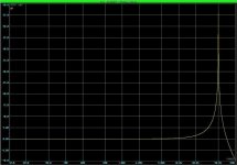
The output filter on the Sony DAV-S400 consists of a 10uH series inductor, with a 1uF to ground LC 2nd order filter on each arm of the HBridge.
I run this though my simulator (Curve below), using the values I measured on my unit. I simulated the input impedance to the LC output filter (PSU + RdsOn) with a nominal 0.2 Ohms per HBridge arm, and with the measured inductance of 10.1uH. I found that at full power 50KHz unload the LC can generate a 56dB Peak at exactly 50KHz! With the output stage being able to swing 54V across the bridge this would result in just over 35000V at the speaker terminals.
What a shame that this Peak is at exactly the spot frequency of 50KHz.
One sure way to fry your girlfriends pesky Cat the next time it tries to chew your expensive speaker cables. So if any of you just happen to leave that DSD test disk repeating the 50KHz 0dB test tone – we on this Post know what your up to!
Unfortunately, however, it’s more then likely that the Capacitors in the LC output filter would fall first before the Cats lovely, sweet precious heart does. So if we find you replacing then with 50kV devices – we REALLY do know what your up to!
How could Sony release a product like this? How much would six sets of Resistors and Caps to damp this resonance cost them?
Does anybody have a solution to the Output filter sensitivity to load issue? It seems there no point in design the output filter for 4 Ohms, as every box speaker I’ve measured has an output impedance greater the 8 Ohms at 20KHz. Notice I said box speakers, and not ESL - my Martin Logins CLSIIz go down to 0.5 Ohms somewhere at HF – no sibilance for me… Er in fact no HF at all for me!
Has John lost the plot again you might rightly ask yourselves – overdosed on the EMC products of his 5MHz 100V output stages?
Despite Jaka’s best influences - not quite yet……
The output filter on the Sony DAV-S400 consists of a 10uH series inductor, with a 1uF to ground LC 2nd order filter on each arm of the HBridge.
I run this though my simulator (Curve below), using the values I measured on my unit. I simulated the input impedance to the LC output filter (PSU + RdsOn) with a nominal 0.2 Ohms per HBridge arm, and with the measured inductance of 10.1uH. I found that at full power 50KHz unload the LC can generate a 56dB Peak at exactly 50KHz! With the output stage being able to swing 54V across the bridge this would result in just over 35000V at the speaker terminals.
What a shame that this Peak is at exactly the spot frequency of 50KHz.
One sure way to fry your girlfriends pesky Cat the next time it tries to chew your expensive speaker cables. So if any of you just happen to leave that DSD test disk repeating the 50KHz 0dB test tone – we on this Post know what your up to!
Unfortunately, however, it’s more then likely that the Capacitors in the LC output filter would fall first before the Cats lovely, sweet precious heart does. So if we find you replacing then with 50kV devices – we REALLY do know what your up to!
How could Sony release a product like this? How much would six sets of Resistors and Caps to damp this resonance cost them?
Does anybody have a solution to the Output filter sensitivity to load issue? It seems there no point in design the output filter for 4 Ohms, as every box speaker I’ve measured has an output impedance greater the 8 Ohms at 20KHz. Notice I said box speakers, and not ESL - my Martin Logins CLSIIz go down to 0.5 Ohms somewhere at HF – no sibilance for me… Er in fact no HF at all for me!
Attachments
Does anybody have a solution to the Output filter sensitivity to load issue?
1.) Linearise your speaker's impedance.
2.) Design the filter according to the intended application.
3.) Use analog class-d amps with after-filter feedback takeoff

Regards
Charles
Hi Charles,
Well many thanks for the ideal, now back to the real world, what about when your designing an amp for “General Consumption” and some Bright Spark "20 something” reviewer try’s it on his favourite box speaker that has an input impedance of 40 Ohms at 20KHz. He then pans your product for “Shrieking like Debbie does Dallas”, whose fault Amp or Speakers – just try telling him that his prize speakers are at fault - the ones he has on "Long Term Loan" after he giving them such a positive review!!
Pls. also note, I accept no liability for anyone’s attempted at making their Cats heart “Beat like a hammer” – keep your DAV-S400 outputs load at all times. I wonder if it’s a common over-sight with Class D amps – some design-notes have the resonance suppress components indicated – most don’t, I sure well fit them after seeing the Sim results.
Hi John,
35kV – no that's not 35000V from Output of Sony DAV-S400.
The second order LC filter is also can be seen like a parallel LC circuit, and the resonant frequency is the same with the crossover freqvency of the filter, from the other sight.
Try some load with the simulator, and it will be parallel with the parallel LC. I think it was calculated to 2 Ohms load.
The modulator's stop band frequency is below the crossover (resonant) frequency. Thus 35 kV will newer venture at the output.
Hi Nagy Gyula,
I think your missing the point, the condition I speak about is only valid if theres no load (speaker) . Its all to easy to leave a speaker disconnected - if you do, theres the risk of some very high voltages develping during a Sign Wave sweep - due to Resonance of the LC, this resonances must be suppressed by an RC network, which Sony don't do in thier DAV-S400.
In the Sony it happens to be at 50KHz, which is a common Freq. to test DSD BW!
As a DSD unit the modulator converters the DSD data to a 192KHz PCM data, it has a (claimed) almost 100KHz BW - and the OP filter is calculated for a 4 Ohm load.
RDSon is very dependent on VGS - consult data books if you still have any doubt - how would you make a linear amplfier if this was not the case? Also why bother with 12V Gate Drive? if a lower voltage would do?
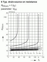
John,
If you see the output characteristic, the upper left area never can be reached with the FET at the given temperature. The characteristic's line from the bottom left point to the constant current (belongs to Ugs at given temperature) near linear -> that's the Rds/on/.
As the temperature rising, the charcteristic curve moves up (at normal currents) -> the Drain-Source voltage drop is rising, that's the positive thermal coefficient. And this phenomenon causes that the Ugs value belongs to a given Drain current is rising (1).
The line is really just 'near' linear, as the drain current is rising and the Ugs is above the treshold voltage, the line is flattening. So the ratio between the Drain-Source voltage drop and the Drain current -> Rds/on/ is rising as the Drain current is increasing.
There is a current value in the data sheets: 'Pulsed Drain Current' or whatever. That range can be reached at such a great Ugs value (if not only greater) you wrote. If Ugs is smaller, the MOSFET is being sweaty.
The Notice (1) demands to sizing the maximum Gate driving voltage such a value what is safely above the maximum threshold voltage for the needed pulsed+static Drain current.
But maybe there's some new under the state of the art. Is there any characteristics like 'Rds/on/ vs. Gate-Source voltage' ?
I think that every half of a H-bridge is calculated to 2 Ohms. From every half the load is seems to be 2 Ohms because of the bridge operation.
Regards,
Hi Jaka,
Many thanks for the picture - thats one BIG fet - I guess not part of your 5MHz 100V OPS What do you switch it with, a car battery?
Any idea (if there's any) how to solve the speaker interface problem?
Timo,
I once had some IXYS samples, but found that the Pd matching was not that good. I normally use short Dead - Times, so Pd matching is very important. One of the better Low-sided Mosfet drivers is the Elantec 7104 - I guess named after one of the worlds Best Scopes - only bettered by the truly brilliant TEK 11302A - which in my mind cannot be beaten by any of today’s "Digital" Scopes for fast pulse work.
Gyula,
Hard to say what the oscillation is due to - I would first suspect the driver - have you tried very small value resisters, say 2R2 right on the Mosfet Gate leads?
Many thanks for the picture - thats one BIG fet - I guess not part of your 5MHz 100V OPS
What do you switch it with, a car battery?Any idea (if there's any) how to solve the speaker interface problem?
Timo,
I once had some IXYS samples, but found that the Pd matching was not that good. I normally use short Dead - Times, so Pd matching is very important. One of the better Low-sided Mosfet drivers is the Elantec 7104 - I guess named after one of the worlds Best Scopes - only bettered by the truly brilliant TEK 11302A - which in my mind cannot be beaten by any of today’s "Digital" Scopes for fast pulse work.
Gyula,
Hard to say what the oscillation is due to - I would first suspect the driver - have you tried very small value resisters, say 2R2 right on the Mosfet Gate leads?
Hi John,
those fets are peanuts. Here is the BIG one I am using.
Regarding filter dampening, possible solutions are:
-resistive dampening, either with series RC connection across filter capacitor as you proposed or with series LR connection across filter inductor. (not a lossless solution, so why use class D?)
-some form of so called PEDEC which would include feedback from filter (why use digital modulator in the first place?)
-use of classBD modulation scheme that is inherent in TAS5015 and achieve inductor ripple cancellation. Move filter resonance at much higher frequencies. Requires use of another 4 fets, but you can use smaller and faster ones. Also complete elimination of common mode noise. Best solution IMHO. Look at this article . I think it has not been patented with digital modulators.
Gyula, I am sorry BCA scheme does not work for you. Maybe you need to increase composite duty cycle of both upper and lower fet over 100%. This seems to be standard solution in analog modulators. Maybe you can do that by increasing turn off delay of the fet drivers. I need to do some simulation before I can give a more definitive answer. I am afraid that I may run at the same problem.
Best regards,
Jaka Racman
Load dependancy
First of all I doubt that the peak under no-load condition would actually be 35 kV, simply due to the fact that you need extremely lossles components to achieve this.
Interesting: The response-peaking at 20 kHz with this extreme peak is still only 2 dB.
It is not that difficult to add a zobel (which every switching amp should have BTW) to dampen that peaking.
It would generally be good practice if all speakers were impedance-linearised within reasonable limits. Not only switching amps and low-feedback amps would profit from it but almost any amp.
The higher the filter cutoff-frequency, the less load dependant is the frequency response within the audio band. The reduced carrier suppression can be dealt with by the use of notch filters (this would of course only work with PWM and not with delta-sigma amps).
Regards
Charles
Hi,
You are right, I was inaccurate but it is also noticeable on the output characteristic that the Drain-to-Source voltage drop is falling with the rising of the Ugs at given temperature . Thank you for setting me to the right way.
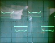
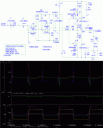
The output waveform is from the "digitalis" circuit, what uses TAS5012 for PWM and little inductance and schottky to the Gate drive. The input 1kHz square wave was converted to discrete values at 44,1 kHz with a Terratec SoundSystem DMX soundcard.
The first noticeable that the ringings are going across a center line about 44 times in a Low-High cycle, at equal intervals. So the ringing is coming from the FIR interpolation filter algorythm of the TAS5012's DSP. None of the interpolators can reconstruct the input signal with plus or minus signed sinusoidal and cosinusoidal waves above the sampling frequency. So the ringing frequency is 22,05 kHz by the sampling theorem. The places of the sampling points is undeterminable on the input waveform, and changing countinously (and maybe periodically) on every input wave. Moreover the number of points on the low and high side is also changing perodically. These conditions bring a little bit dither to the interpolated points. The higher the sampling frequency, the lower the ringing and the dither. Who don't believe, let's simulate the interpolation with software. I written a linear and sinusoidal interpolation simulator in C 2,5 years ago. The result was the same.
Is a solution in TAS5015 to avoid this?
With the BCA I thought to use some IIR filters at the TAS3001 DAP to manipulate the sample values. I think, that the output filter's phase shift is also correctable with these filters, just an inverse filter must be programmed. A circuit schematic should be seen from Crown I-tech.
Regards,
Gyula
You are right, I was inaccurate but it is also noticeable on the output characteristic that the Drain-to-Source voltage drop is falling with the rising of the Ugs at given temperature
. Thank you for setting me to the right way.The output waveform is from the "digitalis" circuit, what uses TAS5012 for PWM and little inductance and schottky to the Gate drive. The input 1kHz square wave was converted to discrete values at 44,1 kHz with a Terratec SoundSystem DMX soundcard.
The first noticeable that the ringings are going across a center line about 44 times in a Low-High cycle, at equal intervals. So the ringing is coming from the FIR interpolation filter algorythm of the TAS5012's DSP. None of the interpolators can reconstruct the input signal with plus or minus signed sinusoidal and cosinusoidal waves above the sampling frequency. So the ringing frequency is 22,05 kHz by the sampling theorem. The places of the sampling points is undeterminable on the input waveform, and changing countinously (and maybe periodically) on every input wave. Moreover the number of points on the low and high side is also changing perodically. These conditions bring a little bit dither to the interpolated points. The higher the sampling frequency, the lower the ringing and the dither. Who don't believe, let's simulate the interpolation with software. I written a linear and sinusoidal interpolation simulator in C 2,5 years ago. The result was the same.
Is a solution in TAS5015 to avoid this?
With the BCA I thought to use some IIR filters at the TAS3001 DAP to manipulate the sample values. I think, that the output filter's phase shift is also correctable with these filters, just an inverse filter must be programmed. A circuit schematic should be seen from Crown I-tech.
Regards,
Gyula
FIR Filter
Hi Gyula,
I'm not familiar with digital filters. Am I right, saying linear phase filters do not exhibit this ringing befor and after transitions? I believe, Linear Technology wrote some interesting stuff in their Application Handbooks.
Attached is a floating driver principle for source-coupled PN-stages. I do not know, if it is already established (McMurphy says: Sure!). May be, John or anybody else can use it.
Regards, Timo
P.S. I have permanent trouble concerning the stability/convergence of the PSpice 8.0 simulator (yes, it is rather old). Is there a suggestion for a stand-alone Spice-compatible simulator for a low budget (private and university usage), which will use the spice-models of the semiconductor manufacturers?
Attachments
- Status
- This old topic is closed. If you want to reopen this topic, contact a moderator using the "Report Post" button.
- Home
- Amplifiers
- Class D
- Anyone interested in a digital amplifier project?