Floating Driver
Hmm, the gif-pictures of the simulation schematic and data were removed (by moderators?). Was there anything wrong?
They are located here now:
http://www.ibtk.de/project/class_d/pspice/ver_0.3/pn_floating_driver_schematic.gif
http://www.ibtk.de/project/class_d/pspice/ver_0.3/pn_floating_driver_data.gif
R118, R99, R101, R106, R100, R98, R110, R119, C39 were inserted, to improve the stability of the simulation.
The coupler (S4, S5) may be an ADuM1100. The gate driver (S1, S2) should have a supply (better: ouput-) voltage of more than 2*Vgs of the MOSFETs. The 'trick' is the doubled bootstrap circuit with D36, D37, C31, C38, referenced to the bridge output.
Regards, Timo
Hi Timo,
attached is driver schematics that was actually tested in a circuit and works well. It uses transformer coupled floating power supply. I tried it with bootstraping power supplies such that you propose, but the result was more noise coupled back to the modulator. If you use bootstraping power supplies, some series resistor or inductor might be in place.
Regarding spice I use Intusoft Ispice, but have heard good things about free LTspice (Linear Technology website) and Simetrix.
Best regards,
Jaka Racman
Attachments
Hi Timo,
I don't remember, I'm going to look after this. I use Electronic Workbench 5.0. It is not good at all, gives amazing results in some conditions when coils are used.
Unfortunately I am also not familiar in digital filters . We studied these filters some years ago, but I don't remember. I planned a recollection in digital signal processing for this summer.
Now I withdraw for some months. Have to begin my external essay. Thank YOU for the good advices!
Good luck for everybody!
Gyula
Hi Jaka,
That’s one weird driver / output configuration, I can see how you solve the cross-conduction issue – very clever! However, I cannot understand how limiting the Current product with the Gate Inductor speeds up the switching. Still need time to get my head around the circuit – maybe a lot of time… Can’t say I ever seen a driver / OPS like this.. very impressive…. at least I think….. It makes my design look very simple and ordinary.
I use Proteus Design from Labcenter Electronics – it comes complete with PCB Layout, Schematic editor and Simulator. Very happy the PCB Layout and Schematic editor, but I’m not that happy with the Simulator. Its great with filters and op-amp type circuits. However, poor when it comes to Fast Pulse circuits and mixed Analogue / Digital circuits such as PWM modulators. I keep getting non-convergence errors etc.
I’ve only been using the Simulator side of the software for a couple of weeks – so I guess I have a lot to learn.
Timo, is the ADuM1100 an Opto-Coupler? I found in the past that opto-couples cause large amounts of Phase Noise and Pulse Width Distortions. I used to use the fast 50MBPS HP’s (I can’t remember there Part #) but gave up due to their poor performance in my application - ended up just Cap coupling.
If the design uses a SRC, then a notch filter seems a very good idea – but I have no idea what the circuit would look like – way too much Math for me
Gyula, Good luck with you course – you know where to find us") I’m sorry I thought the Scope shoot was the output stage switching waveforms – not the audio output. I guess it’s the FIR filter; hard to believe it’s so bad… thankfully, we don’t listen to Square waves that often – but transients? I wonder what effect up-sampling would have, if any? Can you be sure the effect is just the TI digital filter, are you using an ADC on your sound card – or generating the Square waves directly in the digital domain?
I’m sorry I thought the Scope shoot was the output stage switching waveforms – not the audio output. I guess it’s the FIR filter; hard to believe it’s so bad… thankfully, we don’t listen to Square waves that often – but transients? I wonder what effect up-sampling would have, if any? Can you be sure the effect is just the TI digital filter, are you using an ADC on your sound card – or generating the Square waves directly in the digital domain?
Its true that the MOSFET threshold voltage reduces with increasing temperature – but the RdsOn value increases with temperature - if your unlucky this can lead to thermal runaway - even in a Hard Switch design - if your driver stage doesn’t return to zero volts (such as an EF), or your dead-time allowance is incorrect. Low threshold devices are particularly troublesome in this area.
That’s one weird driver / output configuration, I can see how you solve the cross-conduction issue – very clever! However, I cannot understand how limiting the Current product with the Gate Inductor speeds up the switching. Still need time to get my head around the circuit – maybe a lot of time… Can’t say I ever seen a driver / OPS like this.. very impressive…. at least I think….. It makes my design look very simple and ordinary.
I use Proteus Design from Labcenter Electronics – it comes complete with PCB Layout, Schematic editor and Simulator. Very happy the PCB Layout and Schematic editor, but I’m not that happy with the Simulator. Its great with filters and op-amp type circuits. However, poor when it comes to Fast Pulse circuits and mixed Analogue / Digital circuits such as PWM modulators. I keep getting non-convergence errors etc.
I’ve only been using the Simulator side of the software for a couple of weeks – so I guess I have a lot to learn.
Timo, is the ADuM1100 an Opto-Coupler? I found in the past that opto-couples cause large amounts of Phase Noise and Pulse Width Distortions. I used to use the fast 50MBPS HP’s (I can’t remember there Part #) but gave up due to their poor performance in my application - ended up just Cap coupling.
If the design uses a SRC, then a notch filter seems a very good idea – but I have no idea what the circuit would look like – way too much Math for me
Gyula, Good luck with you course – you know where to find us
I’m sorry I thought the Scope shoot was the output stage switching waveforms – not the audio output. I guess it’s the FIR filter; hard to believe it’s so bad… thankfully, we don’t listen to Square waves that often – but transients? I wonder what effect up-sampling would have, if any? Can you be sure the effect is just the TI digital filter, are you using an ADC on your sound card – or generating the Square waves directly in the digital domain?Its true that the MOSFET threshold voltage reduces with increasing temperature – but the RdsOn value increases with temperature - if your unlucky this can lead to thermal runaway - even in a Hard Switch design - if your driver stage doesn’t return to zero volts (such as an EF), or your dead-time allowance is incorrect. Low threshold devices are particularly troublesome in this area.
Hi John,
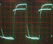
The square wave was sampled with a good soundcard, its coaxial output was connected to the amplifier, and in the amplifier the CS8416 receiver was connected directly to the TAS. Good idea if the soundcard's on-board dsp modified the samples. I will record the samples to .wav and will look at the results. But in my mind it comes from the modulator's interpolator, suspected from the ringings are appear before the transitions too. But this is a good question.
By departing I attach a picture from a square wave what was measured with a 8-bits digital storage scope. In the picture the lower signal is the input, and the bigger is the output with 2 V/division sensitivity at 1 kHz. It captured from the "analog" circuit. Both the input and output signal's quality is very poor with this scope. The circuit uses the AD876 10-bits flash ADC at the input, and its 8 upper bits for modulation. So, this is how a square wave should be appear after the output integrator when there is no interpolation. The integrator's pass-band is at 13 kHz at 12 Ohms load.
The case is similar with the sampled PCM and DSD comparison at this link: http://www.merging.com/2002/html/pyradsd.htm
All of the PCM based formats must use interpolation in order to reconstruct the continuous signal from the discrete values, while the DSD directly records the duty cycles rated by the input signal's actual value, and hereby is getting free from those error sources. I think that every PCM based system can be similar to PWM based DSD if there's no interpolation. This is the case when the PCM values converted directly to PWM signal at the sampling frequency. The "analog" circuit is working in this way, without interpolator, merely not at 2.884 MHz but 125 kHz
I must apologize for my rough tune sometimes on the previous pages!
Best Regards,
Gyula
Attachments
Hi John,
The inductor is really not so important. It merely limits the dissipation in the circuit. You could use resistor or even nothing instead. It addresses the main drawback of the circuit, that by driving both gates at +/- 12V you have to deal with additional GS charge when you drive Nchannel gate negative and Pchannel gate positive. I also noted that by use of the inductor you get much cleaner gate signal (no oscillation at gate threshold plateau whatsoever).
The clever part of the circuit is differentiating transformer signal by using one gate delay (less than 10ns transformer pulses), and then reconstructing gate drive signal by using gate charge of the first complementary mosfet pair.
Only small 2.5 mm toroid with 3 secondary turns is needed. It can be mounted into 2.7mm hole made in the PCB with surface mount pads at both sides for the wire contacts. Very compact design with small coupling capacitance. It also works with 3.3V logic at the input.
Best regards,
Jaka Racman
transformer coupled driver
Hi Jaka,
very interesting, this circuit, seems to be very simple and straightforward. If you drive the HC4050s with 3.3V logic, the transformer should be 1:4, not 4:1, to transform 3V output into 12V, only a misprint.
Is it necessary to prevent the T1 core from saturation?
A member of the german hifi-forum posted, that he had big problems using floating supplies in a similar configuration because of the capacitive coupling of the supply transformer. Full voltage swing will be transferred back to the supply transormer isolation, thus further into the power lines because of the relatively large coupling capacitance (orders of magnitudes higher than that of the driver coupling trafo). In the end they had to change their transformer manufacturer. Keeping this in mind, I would prefer the bootstrap circuit, taking your hints for a decoupling inductance into account. Bootstrapping may hopefully be combined with your circuit.
John, here is the link to the ADuM:
http://www.analog.com/Analog_Root/productPage/productHome/0,2121,ADUM1100,00.html
Their I/O-capacitance is only 1pF, resulting in a transient immunity of 25kV/us.
The 100MBd Agilent HCPL-90xx provide 1.1pF and 15kV/us.
Gyula, I wish you a successful course also.
Regards, Timo
Bootstrapping may hopefully be combined with your circuit.
IMO bootstrapping is the most elegant and straightforward way of supplying power to a high-side driver. There are no problems encountered If there is a restricion on allowable duty-cycle ratios.
If not, then there are still other possibilities to keep contol under continuous-on situations.
Regards
Charles
Hi,
I failed in suggesting the linear phase filters for transmission of square waves without ringing. Seems to be Bessel or simple properly decoupled 1st order RC-networks to exhibit this behaviour.
http://www.linear.com/pdf/dn245f.pdf
In another project I also had to try with filters, including amplification indeed:
http://www.ibtk.de/project/tsm/tc6mainb.jpg
http://www.ibtk.de/project/tsm/tc6_prin.pdf
I found out, that it seems to be impossible, designing analogue high-pass-filters with amplification (also decoupled before or after) without ringing. Each stage will add at least one more peak.
Klein und Hummel have implemented an digital filter in their flagship speaker O500C, which is nerly ideal. I've never seen such good speaker measurement data.
At the end of this text are some literature, which may help for digital filtering:
http://www.kleinundhummel.de/produkte/o500c/dokumente/daga2002-teill1.PDF
Regards, Timo
Hi Timo,
I am afraid you have got the circuit wrong, transformer only has to supply 0.7V to the BE junction of the emitter follower pair. It will not come into saturation , since it only needs to support less than 10ns wide pulses. When i said that the circuit works with 3.3V supply I meant that it can work with other logic families as well. Only requirement is one logic gate delay between both ends of the transformer. I used it directly with the outputs of Altera CPLD. It would also be beneficial to have 3:1 transformer in case of 3.3V logic.
As I pointed out, I have tried my driver with bootstraping and it works. You would also need to add high value resistive divider to power the circuit initially, before the bootstraping kicks in.
Best regards,
Jaka Racman
Oh yes, I have to apologize for my blindness.
A small hint: (vector-)graphics should be converted to and saved as gif, pictures with many colour gradients as jpg, its better fro the presentation quality. I use the free tool IrfanView for it, it is very easy to handle and fast.
Timo
A small hint: (vector-)graphics should be converted to and saved as gif, pictures with many colour gradients as jpg, its better fro the presentation quality. I use the free tool IrfanView for it, it is very easy to handle and fast.
Timo
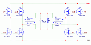
Hi John,
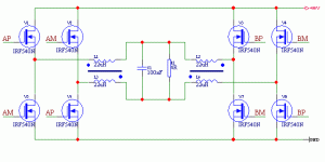
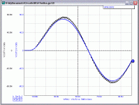
I attached schematic of double bridge output stage that was already proposed. It can be used with classBD outputs of TAS5015 modulator. Filter resonant frequency is 107kHz. Note coupled inductors L1, L3 and L2,L4. They center output common voltage at half of the supply voltage. Next attachment is simulation showing ripple cancelation. It shows 12kHz sine wave burst at 0.93 and 0.001 modulation index. Voltage scale is 20V/div and 20VmV/div. Note almost absolute lack of switching ripple.
I attached schematic of double bridge output stage that was already proposed. It can be used with classBD outputs of TAS5015 modulator. Filter resonant frequency is 107kHz. Note coupled inductors L1, L3 and L2,L4. They center output common voltage at half of the supply voltage. Next attachment is simulation showing ripple cancelation. It shows 12kHz sine wave burst at 0.93 and 0.001 modulation index. Voltage scale is 20V/div and 20VmV/div. Note almost absolute lack of switching ripple.
Attachments
Hi Jaka,
Many thanks for spending the time doing the simulation, the output ripple looks very good - what’s the switching Freq?
Forgive me for some possibly stupid questions – but here goes: -
In simple terms (as that’s how I think), can it be thought of as a double AD output stage (coupled inductors) but with the added benefit of carrier cancellation offered by BD modulation?
1. How sensitive are the coupled inductors to tolerance matching, I once designed a SMPS with coupled inductors for regulation and found it hard to insure QC on the production line (its ALWAYS hard to insure QC on the production line in Asia – but the designs sensitivity to matching didn’t help).
2. Are you sure about the phasing of the Bridge, normally AP and BP are opposite in Phase – what’s to stop them shorting themselves out – or is the current limited by the inductors? So V1 & V7 are on, then V5 & V3. Then sometimes the bridge is in Tri-State – just depending on the 180Deg BD delay shift…. I guess your going to say the inductors limit the current…. In that case, they had better not saturate … (I know inductors should never be allowed to saturate, but in this configuration it would be fatal).
3. What’s the FC of the filter into 4 Ohms, and would you have to double the size of the inductors for 8 Ohms as usual – I’m sure you would…
I also wonder if coupled inductors would cancel the distortion effects due to core permeability linearity verses magnetising current – is there a net constant current in a coupled inductor?
I guess if there is, then the cancellation of the distortion would be dependent on the ratio of the original error and the matching of the coupled inductors. To that end, it maybe an advantage to always use coupled inductors on an AD output stage.
Still thinking about your OPS + Driver (OK call me slow), but there’s more going on then first meets the Eye! Take for example the 10ns transformer coupling… for such narrow pulses I once just used a double-sided PCB as the transformer – no cores.
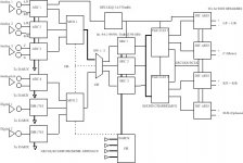
Sorry fellas, but last thing I remember I just finished a 5012/5110. You'r going way too fast for me. But can you have a look at this please (see picture)
6 analog in for 5.1, and extra inputs for dig and analog stereo. Mux this to a SRC and than to tas3103 for channel muxing.
The channels are sent to digital speakers using AES3 balanced stp. The digital speakers will consist of 5015/5182 amps. all running on a vhq HFCLK vcxo @ 98 mhz.
Using tas 3103 for hi/mid/low driver filtering.
Will this work? Especially concerning the clock strategy.
Do the 1703's require their own clock / crystal? Or can they swing on the hfclk available?
Attachments
Hi Pitch 254
1. Is there any reason that you need 2 DIF1703 – I would recommend just Mux the AES inputs to one DIF1703
2. In the “Pre – Amp” section, only the ADC’s need a low jitter Clock, the SRC should be used with the modulator in the Speakers to attenuate the total system jitter. Run each SRC from its own 100MHz clock (using the TAS5015), and not a direct multiple of the sampling frequency.
3. The output DIT's would need to be run off the ADC clock when the unit is in ADC Mode, and likewise, when in AES mode the DIT's should receive their clock from the DIF1703.
I question the need or 6 Analogue surround inputs, would it not be better to received decoded surround data in digital, thus avoiding an extra DAC / ADC loop?
Hi John,
simulation frequency was 390kHz (tas5015@100MHz).Triangular modulator was used for sake of simplicity.
You are correct, it is actually two AD bridges. As you noted, schematic was wrong, correct drive signals are on the picture below. I made error when redrawing simulation schematic in Protel, since Ispice schematics are not readable.
I do not see inductors as critical element. In simulation they were modeled with 0.9 coupling factor. In real circuit, I used toroidal core (both gapped ferrite and Magnetics KoolMu) with one winding on each half of the core. As long as you have equal number of turns on both windings I do not see a problem. My experience with coupled inductors is that it is preferable to have loose coupling, for instance each winding on a bobbin of a UI or UU core. I have tested the circuit with triangle modulators and it works as advertised.
Net current in coupled inductor has the same shape as in single inductor, so no distortion cancellation. So far i have not researched what is the best material for filter core (air?). I know all materials with distributed gap have nonlinear permeability vs AC and DC flux density and frequency and that low mu materials are more linear. But from sharp rise in current when gaped ferrite core comes into saturation I assume that their linearity relative to the DC flux density is superior.
Regarding filter design, it is no different than with single bridge, only that the net inductance is the same as single inductor (22uH) in case of uncoupled inductors. Two paralleled inductors in series with two paralleled inductors. If you couple the inductor, you calculate whole number number of turns for double inductance (44uH), but only half of the output current.
There is one added benefit of coupled inductor. It's transformer action helps to equalize AD bridge switching times.
Regarding driver toroid, I think that air core transformer would not work. You still need to couple several 10's of mA into bases of first bipolar EF pair.
Pitch, I am no expert in digital design, and I know that my first iteration (and the next one or two) of such an ambitious project would not work. I think I will run my DIR1703 from it's own oscillator. I think Brian Brown or some other member would be more competent to comment on this.
Best regards,
Jaka Racman
Attachments
Hi Jaka,
Something has gone wrong with your simulation. The A outputs use positive modulation, while the B outputs use negative modulation. Thus BP similar to AM just toggled in time (with delay). A polarity swapping is needed on the B side. In your way, that's a short circuit.
In this way a simple IRF540 is enough because of the current halfing. The ST's IRF540 has 10 nC miller charge.
The simplier if you use the A and B outpust just for bridge operation.
The band-pass of your filter is at 80 kHz with 30 Ohm.
Regards, Gyula
Hi Gyula,
You are of course correct that L = Al * N^2. But you will also see that circuit with 22uH coupled inductors simulates the same as one with uncoupled 44uH inductors. This is also consistent with your simulation of bandpass of 80khHz (calculated resonance is 75kHz at 44uH). Please, also do not stick to the proposed component values, they were chosen only as the proof of concept. I have built the circuit 3-4 years ago and it was not intended for audio.
Best regards,
Jaka Racman
- Status
- This old topic is closed. If you want to reopen this topic, contact a moderator using the "Report Post" button.
- Home
- Amplifiers
- Class D
- Anyone interested in a digital amplifier project?