Dear All,
Most bridge/parallel PCB designs on this forum use ground planes for the LM chips.
Myself had problems with using ground planes for a LM3886 bridge/parallel design. Of course that can say more about my design skills then about ground planes but when I designed the next version with a consequent star ground THD+N improved highly, and noise get lower. Also the sound quality improved.
Also the National application sheets promote against ground planes.
My personal feeling is ground planes should only be used for digital designs or low-power opamp designs. Not for power amplifiers with high current flows in the ground scheme.
Maybe I am wrong or missed the boat somewhere, that is why I ask to share some thoughts. Pro’s and con’s for a ground plane. I also wonder why the designers on this forum decided to use ground planes for their LM3886 design.
With best regards,
Bas
Most bridge/parallel PCB designs on this forum use ground planes for the LM chips.
Myself had problems with using ground planes for a LM3886 bridge/parallel design. Of course that can say more about my design skills then about ground planes
but when I designed the next version with a consequent star ground THD+N improved highly, and noise get lower. Also the sound quality improved.Also the National application sheets promote against ground planes.
My personal feeling is ground planes should only be used for digital designs or low-power opamp designs. Not for power amplifiers with high current flows in the ground scheme.
Maybe I am wrong or missed the boat somewhere, that is why I ask to share some thoughts. Pro’s and con’s for a ground plane. I also wonder why the designers on this forum decided to use ground planes for their LM3886 design.
With best regards,
Bas
I have recently been spending quite a bit of time thinking about the same question.
see: http://www.diyaudio.com/forums/showthread.php?s=&threadid=138482&pagenumber=2
If a star ground showed improvement, my understanding is that high and low power grounds were likely being mixed (close to a sensitive circuit/component). One possible solution (instead of a pure star ground) is to use two or more different planes for high and low power parts of the circuit and then bring the planes together at a star.
One possible problem that pure star grounds can cause is high trace impedance because star grounds inevitably require many individual traces and space constraints may force the traces to be thin. Thin traces can cause the trace impedance to be significant.
Trace impedance is solely determined by its length, not by its width. Trace width is good for low trace resistance, but increases capacitance.
The ideal ground has a potential of 0 V. A real PCB ground does not have that potential due to resistance of leads and traces from the power suppply. The higher the current the more voltage drops across those resistances and the further away from zero is the ground potential on the PCB. If you have a common ground for power and input, the input ground potential will change with the output current, changing the reference for the amplifier all the time. Therefore you should try to move the common grounding point as near as possible to the point of the lowest (and most stable) potential. Usually that is either slightly behind the main smoothing capacitors in the power supply or the point, where PE enters your amplifier. It can also be the RCA connector, depending on the layout of the other components.
A ground plane is good for low power applications, because the low currents there don't lead to a significant change in the PCB's ground potential.
My impression is that the designers, who use planes for chipamps do it for aesthetic rather than technical reasons.
My impression is that the non-experts, who use planes for any circuit, do not know what they are doing and further do not know why the ground plane does not work as expected.pacificblue said:
My impression is that the designers, who use planes for chipamps do it for aesthetic rather than technical reasons.
In my experience, neither design practice is panacea. We have had a mixed signal telecoms design at work, which used split analog and digital ground planes, suffer bad signal integrity problems. This can easily happen in practice, because often systems need to connect to the outside world at more than one point, e.g. power connector, various input/output connectors etc. And this is where split ground planes can actually do a lot more harm than good, by letting 'dirty' currents flow through sensitive circuit areas. In such instances, a solid ground plane is much preferred, although it is extremely difficult to eliminate circulating currents completely.
Star earthing is good as long as the ground trace impedances can be kept negligibly small for the job, and again no circulating currents are introduced by wrong start-earthing point locations.
In either case, one has to think very hard where unwanted currents could flow from connections to the outside environment and how to stop these from being added to the low-level signals.
Tough one!
Dear All,
Thanks for the input so far.
I think the main problem with ground planes for a BPA300 design is the fact that as well the high current output stage as the analogue inputs (since in all designs so far analogue signal is unbalanced internally and the chip inputs refer to ground) refer all the to the same ground.
Measurements turned out that PSU current flows get modulated at the line inputs from the chips which all refer to the same ground plane. And that explains for me what the THD+N ratio drop significant.
In one post above someone offer the option to use different groundplanes for power and line. In multilayer circuits this is a way to go. One ground plane for power, and one ground plane for line level and e separate ground return for the output. And those all joined together at the best common point closest to zero volts.
Other solutions would be to make the internal line signals balanced truth differential and floating above ground. Some virtual ground circuits for line applications would serve very well too.
The Jeff Rowland LM3886 design use ground planes with very good result.
With best regards,
Bas
I think the main reason not to use a ground plane is that it is really hard to do right with only 2 layers to work with.
One advantage of a ground plane is the high-Q distributed capacitance. This makes for pretty good filtering of extremely high frequencies, but that's not really important for audio. Of course you don't actually want this capacitance to appear everywhere. You can fix that by removing the ground plane from underneath the affected tracks, but then you compromise that other advantage of a ground plane - low inductance.
I thought I had a bunch of links to useful articles about this sort of thing, but I can only find one, and it's not specific to the low-frequency analogue that we are interested in.
it has been suggested in another thread here on diyaudio to use a combination of star and a plane:
http://www.diyaudio.com/forums/showthread.php?postid=887542#post887542
what do you think of the above idea?
Also, i recently designed two pcb's, one with a star ground and one with a ground plane, for a simple power supply built around 3 pin adjustable regulators. Which would you pick and why?
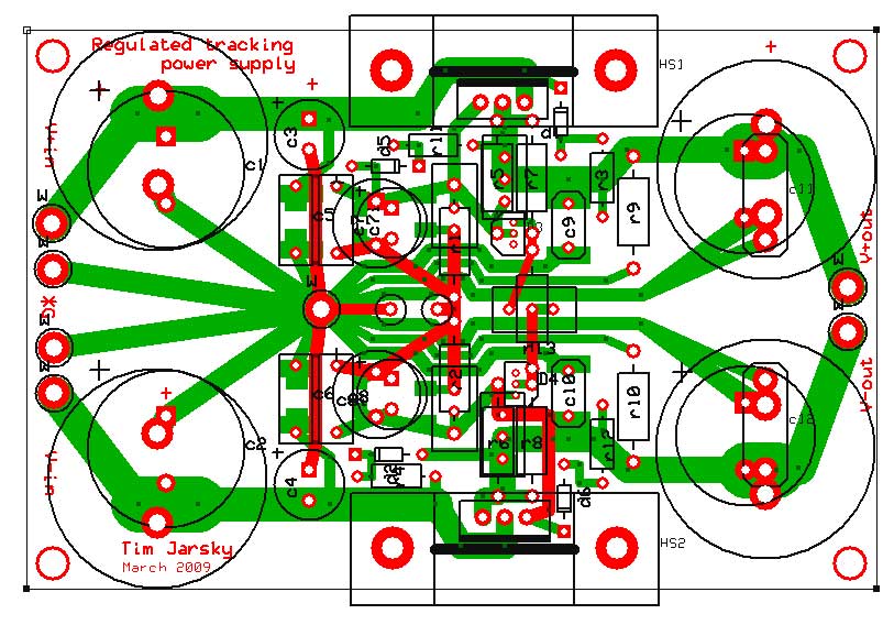
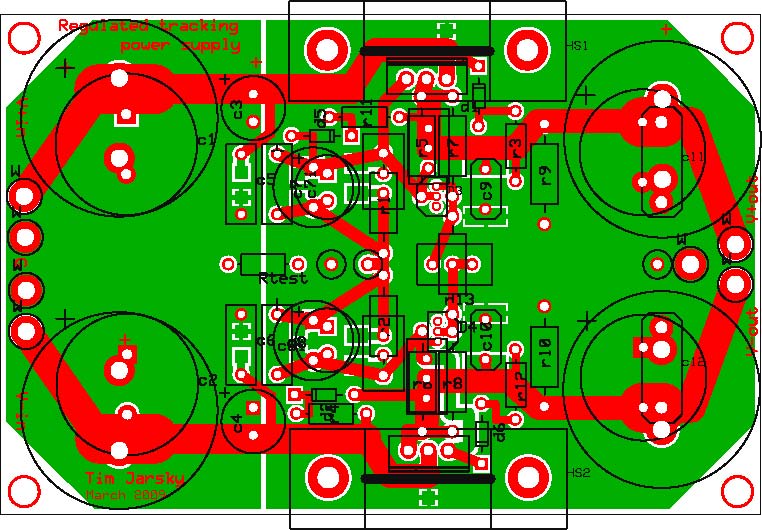
** for the purpose of this discussion please ignore the slice in the ground plane. i placed that there to allow for experimentation.
http://www.diyaudio.com/forums/showthread.php?postid=887542#post887542
what do you think of the above idea?
Also, i recently designed two pcb's, one with a star ground and one with a ground plane, for a simple power supply built around 3 pin adjustable regulators. Which would you pick and why?
** for the purpose of this discussion please ignore the slice in the ground plane. i placed that there to allow for experimentation.
Decide first, which components you actually use, then optimize the layout for them. Too many options for a certain component means too many compromises.
Then decide, if you want to use planes or not. If you use planes, use them for the V+ and V- potentials as well.
If you don't use planes, in a power supply you want the traces as wide as possible to keep trace resistance (= temperature rise) low. So make the V+, V- and Gnd traces wider up to the point, where they look like planes, but don't pass the planes above and below each other, and keep some distance between them. Something like a mix of your two designs. That means V+, V- and GND will all be on the bottom layer, the V+ and V- planes extend up to the board edges, and the ground plane remains within the limits formed by the V+ and V- planes.
Move the big electrolytics as close as possible towards each other, so that resistance and inductance between them on the ground trace/plane becomes as small as possible.
Don't you need a ground connection at the output? The PCB ground is the reference for the regulators, therefore all components that you connect to them, should reference their power supply ground pins to it as well and it should become your star point for that purpose.
pacificblue said:Decide first, which components you actually use, then optimize the layout for them. Too many options for a certain component means too many compromises.
Then decide, if you want to use planes or not. If you use planes, use them for the V+ and V- potentials as well.
For the moment i want to respond to your first two comments. It is definitely true that i have a few to many options. In the version i ordered i have a couple less options than what i am showing in the above pictures. I should mention that i do have a lot of options because it is an experimental board - the final version will just contain the parts necessary for optimal performance. Also, it is only experimental in the sense that i plan to use it to test the effects of various configurations so that I can do some hands on learning. A more experienced person might see most of my tests as rudimentary and consequently a waste of time.
I am having a hard time visualizing how to implement planes for the V+ and V- in addition to the ground. Wouldn't this require 4 different planes: V+in, V-in, V+out, and V-out? Also the pin arrangement of the voltage regulators would require that the planes for V+in and V+out overlap which is not possible with just a two layered board. Would you then recommend having the planes meet near the voltage regulator and then have discrete traces running from the plane to the appropriate pin?
I'll try to address your other helpful comments when i get a chance later today. Thanks for your help.
I havent been into this for much more than a year, but i am working as a traineee in a company which makes all sorts of wireless communication links, phones, bluetooth things and so on.
I have been so lucky to have been working with designing a 100W RF generator, for two reasons, there is SO much to learn in designing such a thing, and one gets a good feeling about grounding.
However, this was designed to be a 4 layer print, but never the less.
I was told to find out which was best, star grounding and groundplaning.
Star grounding because i could make the print inhouse for "free" (a frew pennies).
But, i must say that it just didnt work too well.
I thought that it might be because of the high frequencies, and yes, that had alot to do with it. But my most recent pa150 lm3876 amp had the same problems.
I knew where the power came from, but the leads for my small caps just couldent do the job, no matter what i did. So i decided to use 10 times the time to make my design at a 2 layer print, and then optimize the layout for a good groundplane. And i have no troubles with noise of any sort.
So in my experience the groundplane is the best.
But with that said, i might add that, as with all other electronics, it will bee good but never great, if you dont know what you are doing. So if you feel comfortable with star grounding, then do that. But dont discard the other, use the time to learn what the two different ways of grounding has to offer.
In relation to the talk about seperating the signal ground and pwr ground, it is a good idea, i have had a great deal of luck with that as well.
I used a buffer preamp before the 3xlm3876, and the supply for that was as well not directly connected to the pwr supply. I made a DC shorted low-pass filter between them. And that works wonders.
Someone in here who had the same experience?
I have been so lucky to have been working with designing a 100W RF generator, for two reasons, there is SO much to learn in designing such a thing, and one gets a good feeling about grounding
. However, this was designed to be a 4 layer print, but never the less.
I was told to find out which was best, star grounding and groundplaning.
Star grounding because i could make the print inhouse for "free" (a frew pennies).
But, i must say that it just didnt work too well.
I thought that it might be because of the high frequencies, and yes, that had alot to do with it. But my most recent pa150 lm3876 amp had the same problems.
I knew where the power came from, but the leads for my small caps just couldent do the job, no matter what i did. So i decided to use 10 times the time to make my design at a 2 layer print, and then optimize the layout for a good groundplane. And i have no troubles with noise of any sort.
So in my experience the groundplane is the best.
But with that said, i might add that, as with all other electronics, it will bee good but never great, if you dont know what you are doing. So if you feel comfortable with star grounding, then do that. But dont discard the other, use the time to learn what the two different ways of grounding has to offer.
In relation to the talk about seperating the signal ground and pwr ground, it is a good idea, i have had a great deal of luck with that as well.
I used a buffer preamp before the 3xlm3876, and the supply for that was as well not directly connected to the pwr supply. I made a DC shorted low-pass filter between them. And that works wonders.
Someone in here who had the same experience?
Why do it like that? If you have the ground traces follow underneath V+/V- then you get lower inductance (due to decreased loop area), plus the extra capacitive coupling.pacificblue said:...but don't pass the planes above and below each other, and keep some distance between them. Something like a mix of your two designs. That means V+, V- and GND will all be on the bottom layer, the V+ and V- planes extend up to the board edges, and the ground plane remains within the limits formed by the V+ and V- planes...
Yes, to all.okapi said:I am having a hard time visualizing how to implement planes for the V+ and V- in addition to the ground. Wouldn't this require 4 different planes: V+in, V-in, V+out, and V-out? Also the pin arrangement of the voltage regulators would require that the planes for V+in and V+out overlap which is not possible with just a two layered board. Would you then recommend having the planes meet near the voltage regulator and then have discrete traces running from the plane to the appropriate pin?
If you prefer it like that, you should probably use planes to start with.Mr Evil said:Why do it like that? If you have the ground traces follow underneath V+/V- then you get lower inductance (due to decreased loop area), plus the extra capacitive coupling.
pacificblue said:
Yes, to all.
If you prefer it like that, you should probably use planes to start with.
Thanks to diyaudio forum member Marce i was made aware of the following article:
Constructing your Power Supply - Layout Considerations, by Robert Kollman
It is a great article and it served to demystify pcb design quite a bit.
On page 4-5 last paragraph it says the following:
"It should be noted that the effectiveness of the ground plane depends upon it being significantly wider than the trace above it. For example, if the ground plane were the same width as the trace above it in Fig. 7, the resulting symmetrical conductor pair has a total inductance per unit length slightly greater than the value calculated by the formula of Fig. 7. However, this total inductance value is distributed so that one half appears in series with each conductor. Thus, the lower conductor is no longer an effective ground plane. When the lower conductor is made significantly wider, the asymmetrical structure causes almost all of the total inductance to appear in series with the smaller conductor, thereby minimizing the impedance in series with the wider ground plane. "
The article also provides a formulas to calculate Trace inductance (Fig 6 and 7). In both cases trace inductance is critically dependent on trace width.
So it seems that the second design i posted, the one with the ground plane on one side and individual traces on the other, with respect to trace inductance, may in fact be the best choice.
A large plane below/above many components and high impedance nodes could increase parasitic capacitances so much that performance is worse, than when using correctly placed traces.
Ground planes and power planes are rarely of any benefit for signal processing of audio frequencies.
Ground and power planes become very useful for lowering power impedances in very high frequency processing, as in the PCB for a 2GHz CPU computer.
Ground planes and power planes are rarely of any benefit for signal processing of audio frequencies.
Ground and power planes become very useful for lowering power impedances in very high frequency processing, as in the PCB for a 2GHz CPU computer.
Last edited:
Trace impedance is solely determined by its length, not by its width. Trace width is good for low trace resistance, but increases capacitance.
Why or how does a wide trace increase capacitance? Only if there's a ground plane on the other side of the board.
- Status
- This old topic is closed. If you want to reopen this topic, contact a moderator using the "Report Post" button.
- Home
- Amplifiers
- Chip Amps
- star ground vs. ground plane