This obsession with star spindly legged star ground seems to be only in the DIY audio arena, don't see it in professional audio, instrumentation or any other field of electronics.
Hello!
Well, on a French forum we have this guy who came to visit, and he did a board with a MCU controlling a PWM MOSFET for a heating element. And because he was afraid of the noise coming from the power bits, he added an isolator between the two, with nice split ground planes and all... for no reason, since everything is already powered from an isolated switching power supply. I think the two grounds on the two sides of the isolator are connected somewhere.
Then came the ESD gun test: isolator exceeded dV/dt rating and did nasty things.
Well. I respect the guy: the eggheads up above forced him to use 500kHz PWM to control a heating element due to some obscure ego-politico-marketing reasons, and the thing only fails most of the EMI testing by "a little bit".
Today I have been laying out a PCB for an LT1932 LED driver, which runs at 1.2MHz, and the datasheet says...I am not aware of any ICs that are designed specifically for use with a ground plane and other ICs that are designed to be used only with a star ground...
always use a ground plane under the switching regulator to minimize interplane coupling.
It's a switcher that relies on harmonics probably going out beyond 12MHz.Today I have been laying out a PCB for an LT1932 LED driver, which runs at 1.2MHz, and the datasheet says
It NEEDS low impedance at these frequencies to work properly.
That duty demands the planes that Marce reminds us work at HF. And probably not just a ground plane but power planes and may be signaling ground plane separate from the power ground plane.
Today I have been laying out a PCB for an LT1932 LED driver, which runs at 1.2MHz, and the datasheet says
What Tom is saying is a chip is a chip, its up to the designer to decide on the topology of the layout...
Schematics and grounding schemes are nice. Still, I prefer real world examples.
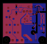
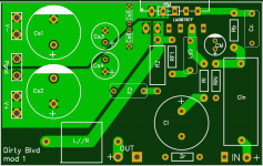
Here's a layout for a very simple lm3886 board (under 5*5 cm). It's heavily inspired by Tomchr's suggestions in various threads.
It's a mix of groundplane use and star grounding at the output connector.
ps: c6 should be bipolar and the extra ground connector is used to connect a groundloop breaker to PE.
Attachments
True,insted of c2 220k put 22k but then u need increase c1.excess avoidable output offset !
+IN sees 222k and -IN sees 22k
That will give an output offset.
I agree. The values used don't make much sense !True,insted of c2 220k put 22k but then u need increase c1.
and that applies all around the sch, not just the input impedance.
The schematic was only posted to reference the parts numbers/position. As already said above, it's the result of a quick copy-paste job (the input section values made sense when there was a non inverting opamp buffer before the lm3886).
The part of interest to the thread is only the layout.
The part of interest to the thread is only the layout.
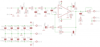
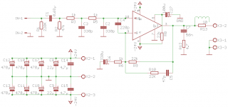
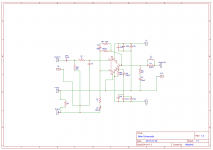
Since some asked for a schematic with correct values, here it is.
Justification for the important stuff:
R2: 47K. A compromise between output offset and input impedance. Can be reduced to 22K if wanted.
C1: 0.68µF. With R2, set the -3db point of the input filter at about 5Hz.
R6-R9: 1K-22K. Set the gain at about 27db. High enough to gain some stability margin.
C6: 330µF. Set the -3db point at 0.5Hz, reducing interaction with the input filter.
The rest should be self explanatory.
Attachments
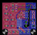
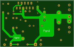
I tried to summarize the recommendations by Mark, Andrew, and Tom - thankU for your always great support - and I had this layout! Rm and Rf are directly on the IC legs. Grounds are on the bottom side. Sgnd is linked to Pgnd via 2r (optional). What do you think?
Marco
Marco
Attachments
- Status
- This old topic is closed. If you want to reopen this topic, contact a moderator using the "Report Post" button.
- Home
- Amplifiers
- Chip Amps
- star ground vs. ground plane