Yes, you are right. I missed the "long" word.
I was looking at the violet THD and the wrong schematic.
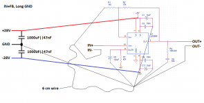
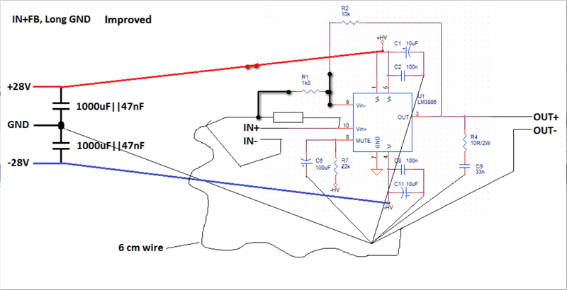
At least now it makes sense to me that the lowest THD would be the one where the NFB goes directly to the star. Though I missed why the 6cm wire is necessary.
AFAIK (or guess), the only ground not carrying any current is the NFB, and it should be connected to a Reference Ground. All the others seem to me that they go to Power ground, or a ground plane.
I was looking at the violet THD and the wrong schematic.
At least now it makes sense to me that the lowest THD would be the one where the NFB goes directly to the star. Though I missed why the 6cm wire is necessary.
AFAIK (or guess), the only ground not carrying any current is the NFB, and it should be connected to a Reference Ground. All the others seem to me that they go to Power ground, or a ground plane.
If you can get people to think about grounds rather than asking for simple recipes (and implementing them badly) then that is good.
Yep. Thinking and understanding is good.
Tom
AFAIK (or guess), the only ground not carrying any current is the NFB, and it should be connected to a Reference Ground. All the others seem to me that they go to Power ground, or a ground plane.
All returns (GNDs) carry current. The input current returns to the source. The feedback current returns to the power supply capacitors.
You should show the polarizing resistor of Vin+.
It should be connected to the left of R1 by the shortest distance because every voltage induced between them is going to be amplified.
And only then, you can link their common point to the point which you think to be the best 0V reference.
I found copper pours very important in high impedance valve stages.Ground planes and power planes are rarely of any benefit for signal processing of audio frequencies.
.
I was getting pick up of the HVAC (160VAC) signal without a copper pour.
Ground planes make great shields against capacitive coupling. For example, I built Sam Gröner's low noise measurement preamp, two channels on the same PCB. In retrospect, I made a mistake : I should have put one channel on top and the other channel on the bottom. This would have resulted in lower crosstalk, as the ground plane would have shielded one channel from the other. In my implementation, the big capacitor at the input of channel 2 did pick up the output signal of channel 1 simply by being close to it. Big film caps couple capacitively to everything around. Copper foil helped solve the issue.
As for the above schematic, the fact it works better with a 6cm GND wire is a bit mystical to me.
I'm perfectly OK with the schematic in this post having lower performance ; the solder joint between the two large capacitors is a very noisy place and you don't want to use it as a star.
But why 6cm and not 1cm or 5mm? I mean, hmmmm.....
Last edited:
you can follow the currents, see "clean" vs "dirty
just have to add impedance guesstimates, actually test hierarchical gnd schemes in sim
measuring hardware will show when your conceptualization failed
try putting Av 4000 stain gage amps and 16 bit ADC within inches of 100 MHz uC, DSP - you could learn a lot about board gnd partitioning
just have to add impedance guesstimates, actually test hierarchical gnd schemes in sim
measuring hardware will show when your conceptualization failed
try putting Av 4000 stain gage amps and 16 bit ADC within inches of 100 MHz uC, DSP - you could learn a lot about board gnd partitioning
yes a "star", by itself, is exactly a "too simple" idea
hierarchical grounding, "dirty"/"clean" branch separation are important ideas too
and like DF says - CT to reservoir cap junction is "dirty" - has rectified charging current pulsing in the wire, creating nasty nonlinear Vdrop in its R,L
the mains xfmr secondary is floating, the isolation should be taken advantage of by letting it be an "open" end of the dirty current branch
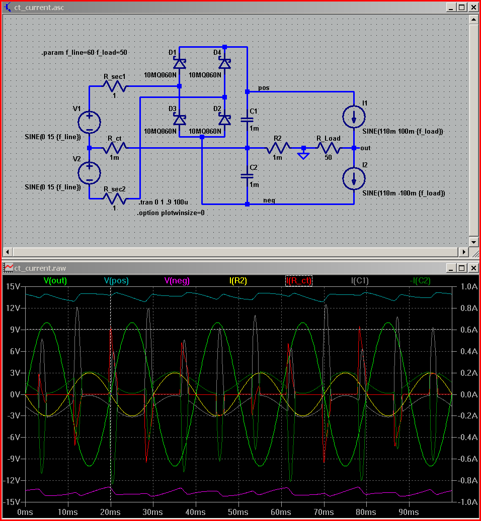
at the very least the location of the "star" point can be chosen for better or worse performance - and worse would be the xfmr CT
................
But why 6cm and not 1cm or 5mm? I mean, hmmmm.....
Who says it is the length? Diameter sounds more logical for low impedance...

try putting Av 4000 stain gage amps and 16 bit ADC within inches of 100 MHz uC, DSP - you could learn a lot about board gnd partitioning
Throw in a few DC-DC converters in close proximity for extra good karma

Which means many people are following that and having higher THD.
Exactly.
There can be big issues when a Reference is connected to a noisy Ground plane, thus any process depending on a clean Ref will be severely affected.
Throw in a few DC-DC converters in close proximity for extra good karma
And USB PHY Receivers and PDN as well...
You should show the polarizing resistor of Vin+.
It should be connected to the left of R1 by the shortest distance because every voltage induced between them is going to be amplified.
And only then, you can link their common point to the point which you think to be the best 0V reference.
Agreed. That is why I said that important parts were missing from the schematic: the input resistor and the RFI filter. Tom adds them on his side schematic, though not specified.
Mark, why do you say that the feedback current returns to the power supply capacitors? The THD for not retuning there is better.
Mark, why do you say that the feedback current returns to the power supply capacitors? The THD for not retuning there is better.
Feedback is a portion of the output signal, ergo its current has to return to the same place as the output return.
OTOH, it is used as a voltage reference for the diff amp and becomes slightly tricky to actually implement.
It effectively needs low impedance to both the high current and voltage reference 'grounds'. The use of trickery such as small resistors separating the two 'grounds' is one way to achieve this, as long as the resistor value is very small compared to Ri.
Another way to do this is a very careful layout. Bundling everything into a star or dumping all of the nodes on a plane without thinking about the currents is not going to work well.
I think you are saying that the lower end of the NFB goes to the Decoupling Ground on the amp PCB.Carlmart, you connect the feedback return to the output return. The current just returns to the capacitors via the ground plane.
Is that correct?

And IN- should not be connected to a big single wire loop.
It should be connected directly to the junction between R1 and the unlabelled (Rin)
We are trying to minimise the loop areas to minimise the pick up of interference.
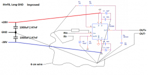
This now looks very much different from
It should be connected directly to the junction between R1 and the unlabelled (Rin)
We are trying to minimise the loop areas to minimise the pick up of interference.
This now looks very much different from
connect the feedback return to the output return
- Status
- This old topic is closed. If you want to reopen this topic, contact a moderator using the "Report Post" button.
- Home
- Amplifiers
- Chip Amps
- star ground vs. ground plane