The only places where parasitic capacitance is a problem are (very) high impedance nodes. In most audio designs, you can identify quite easily the problematic ones. The input pins of an opamp for example. Have a look at the tpa6120a2 evaluation board to see how you can have a groundplane with some cutouts at the sensitive points. Best of both worlds.
Most eval board for audio use groundplanes (and powerplanes) these days, even for analog. Even at audio frequencies, pours allow a lower impedance return, simply by throwing more copper at it.
Most eval board for audio use groundplanes (and powerplanes) these days, even for analog. Even at audio frequencies, pours allow a lower impedance return, simply by throwing more copper at it.
What I mean is not ground or power planes, because I'm not sure they are necessary, except on digital or on low noise high gain circuits.
What I mean is leaving separation between tracks, any tracks, at a minimum (to be specified) and make them as wide as possible. If you have several joined soldering points, I make what I call an "island" with them, that would also allow some latitude when using through hole parts with different size, or even for using SMD parts on the copper, because of the copper sides being close by.
I usually draw my PCB designs for the parts to be as close as possible, which I think is most important, joining everything with standard 1mm/2mm traces. Then I widen up everything, to fill up or pour copper together in "islands".
Of course I'm concerned with parasitic capacitance, which I think is a more serious problem with double-sided designs, which are now mostly the norm.
What should you do on inputs pins then and what other areas should we concern with on a discrete or IC preamp or power amp then?
I suggest reading the first 50-or-so posts in this thread: http://www.diyaudio.com/forums/chip-amps/252436-lm3886-pcb-vs-point-point-data.html
You can also see my simulation methodology on my website: LM3886 chip amp grounding.
The key to good grounding is a low ground impedance. The lowest impedance you can get is with a plane, thus, the plane will provide the best performance - IF DONE CORRECTLY! There are certainly ways to screw up a ground plane. You need to keep the quiet parts of the circuit on parts of the plane that has the lowest current density, or set up a reference plane.
My LM3886 Done Right uses a ground plane for the high currents and a reference plane for the quiet nodes. The two join in one spot and one spot only. The location of this spot is critical. It needs to be at the output connector. I provide the justification and simulation results on my Taming the LM3886 website and the data in the LM3886 P2P vs PCB thread linked to above.
A star ground provides the highest ground impedance possible, thus, is guaranteed to provide the worst performance. I've had several circuits with star ground that couldn't even meet the data sheet specs of the LM3886. My LM3886DR measures slightly better than the data sheet figures.
Tom
Hi Tom,
Very interesting findings on THD on the several grounding groupings & arrangements. The lowest THD schematic looks like a basic arrangement for any power amp or preamp.
http://www.diyaudio.com/forums/atta...int-point-data-lm3886_p2p_layout_inpfbgnd.png
The one I had been using till now was the one you called "star ground", but it was decoupled by a 10R series resistor.
Now please tell me how a ground plane would help there or why the "island" arrangement I suggested above could jeopardize THD or anything. Am I missing something?
There are two issues at play here :
1) Ground plane is good because it reduces impedance of GND. It also allows proper decoupling of power supplies, acts as shield, reduces emissions and pickup, etc. No question about this.
2) Problem: the designer is now tempted to use this ground plane as a 0V reference, and this opens a new can of worms, because currents are flowing through it, therefore GND potential will be different depending on where you probe.
So, when something is connected to "GND", always ask yourself : am I using GND as a 0V reference ? The problem isn't the ground plane itself, the problem is temptation to use it as a voltage reference. You must resissstttt.....
- Classic Star GND is a way to trade off GND impedance (which becomes enormous) for a cleaner reference (at very low frequencies) by manually enforcing proper current paths.
- If you are using GND as 0V reference, then everything that is connected to GND, especially decoupling caps*, must be prevented to inject distorted current into GND. And your GND plane must be cleverly contoured (as Tom did) to guide high currents away from sensitive spots. You end up with several planes connected in a star. It works.
- Other solution is to use differential amplifier, substracting amps etc, as M. Putzeys did in "The G Word" which is also a good idea.
- Both can also be combined.
*: Example : let's consider an opamp.
Input current = 0
Output current = undistorted signal (therefore we don't care if a little bit of it crosstalks into the next stage via GND modulation)
Therefore, good old Kirchhoff says that, whatever the currents drawn by the opamps' supplies, even if it goes into class B, their sum is equal to the output current, and thus undistorted. Therefore, if we connect both this opamp's decoupling caps to GND at the same point, no distorted signal will be injected into GND.
And your GND plane must be cleverly contoured (as Tom did) to guide high currents away from sensitive spots. You end up with several planes connected in a star. It works.
Several planes, several traces or several wires?
On Tom's example, the measured amplifier was P2P, if I'm not wrong.
Was that same arrangement later converted into a pcb, with a ground plane? Are there THD graphs for that pcb too which we can compare? Did THD improve or the amp sounded better?
Yes, see: www.diyaudio.com/forums/vendors-baz...ht-45-w-8-0-002-thd-n-80-w-4-0-004-thd-n.htmlSeveral planes, several traces or several wires?
On Tom's example, the measured amplifier was P2P, if I'm not wrong.
Was that same arrangement later converted into a pcb, with a ground plane? Are there THD graphs for that pcb too which we can compare? Did THD improve or the amp sounded better?
Several planes, several traces or several wires?
Probably a mix of the three if your gear is split into several boards.
On Tom's example, the measured amplifier was P2P, if I'm not wrong.
I was referring to Modulus-86, the ground layout on this board is excellent.
Now please tell me how a ground plane would help there or why the "island" arrangement I suggested above could jeopardize THD or anything.
You have received several responses that all say the same thing, including the one you replied to (Post #24). I suggest re-reading those along with the references linked to.
The key to good performance is LOW GROUND IMPEDANCE.
The lowest impedance possible is the one you get with a ground plane. Therefore, if you want good performance, use a ground plane.
Now the issue is that you have a couple of sensitive nodes that connect to ground. You do not want to impose an error voltage onto these nodes. I call those nodes the reference ground (or signal ground). Again: Low impedance is key, but as the reference ground generally doesn't carry much current (current returned by the input network), you can live with a slightly higher ground impedance here. While a plane would be ideal, a pour generally works just as well and leaves some room for the other traces.
The two grounds (power ground and reference ground) need to connect in one spot. The optimal spot is the ground connection at the speaker output. You can see why on my website (linked to in Post #24).
A spider ground or excessive moating of the ground plane maximizes the ground impedance, thereby, minimizing performance. That's not what you want to do if you want performance.
Tom
Tom and peufeu,
Lesson 1. Main objective: target for low ground impedance.
Lesson 2. A ground plane is the best solution to get LGI.
Lesson 3. Finding and organizing sensitive nodes grounding.
Lesson 4. A pour can replace a ground plane to simplify design in reference/signal ground nodes.
Lesson 5. power ground and reference ground need to connect at one spot only.
Lesson 6. Optimal spot (Main star?) is speaker output.
This what I have learned until now. Let's see if I can implement that on a real circuit and put it here. Would you comment on that if I do?
These two sentences say opposite things. Only the second sentence is correct.pacificblue said:Trace impedance is solely determined by its length, not by its width. Trace width is good for low trace resistance, but increases capacitance.
Yes. Ground planes for RF and digital; bus or star for analogue audio - I prefer bus.AndrewT said:Ground planes and power planes are rarely of any benefit for signal processing of audio frequencies.
Ground and power planes become very useful for lowering power impedances in very high frequency processing, as in the PCB for a 2GHz CPU computer.
There are always other conductors somewhere. Wider traces mean more capacitance and smaller inductance, other things being equal.carlmart said:Why or how does a wide trace increase capacitance? Only if there's a ground plane on the other side of the board.
No. Low ground impedance is a key, not the key. Also important, perhaps more important, is knowing where the currents flow. A ground plane hides this. Of course, if a chip was designed to use a ground plane then it might work best on a ground plane. This does not mean that 'ground plane is best'; it means 'ground plane is best for chips designed to use a ground plane'.tomchr said:The key to good grounding is a low ground impedance.
There are two keys to good grounding:
1. knowing that currents always flow in loops - know where your currents flow
2. knowing that voltages always exist between two points (never one or three) - know where your 'voltages' are referenced to
No. Low ground impedance is a key, not the key. Also important, perhaps more important, is knowing where the currents flow. A ground plane hides this.
No, not really. In a ground plane you'll have varying current densities. You can get a pretty decent handle on those current densities by estimating the resistances between points on the plane. For the full picture you'll need a field solver or some other tool.
Of course, if a chip was designed to use a ground plane then it might work best on a ground plane.
All IC design I have done has been from the pins and inward. It was assumed that the customer or end user/designer was skilled in the art of electronics, hence, knew how to get the most out of the IC, thereby achieving the data sheet performance.
As an IC designer I had no influence on what the customer did. If the customer chose to shoot him/herself in the foot by using a crappy PCB layout that was really their problem. Of course, the customer quickly shifted the problem to our applications engineers who then proceeded to explain how to use the chip to get the maximum performance out of it. Here's a pro tip for you: Read the application section of the data sheet!
Aside from maybe ICs that require a thermal connection to a plane, I am not aware of any ICs that are designed specifically for use with a ground plane and other ICs that are designed to be used only with a star ground. It would be marketing suicide to do so. Maybe some 10+ GHz RF ICs or something assume the presence of a ground plane. Nothing that pertains to analog that I know of does.
There are two keys to good grounding:
1. knowing that currents always flow in loops - know where your currents flow
2. knowing that voltages always exist between two points (never one or three) - know where your 'voltages' are referenced to
Correct. To minimize the voltages in (2) above, the impedance of the ground needs to be minimized. That's Ohm's law. As I've said repeatedly, the lowest impedance is a plane.
As I have also said repeatedly, put the high currents on a ground plane and the sensitive nodes on another ground plane (or pour if you can't afford the real estate for a plane). Join the two grounds at one spot and one spot only.
Following these two suggestions meets both of your points (1) and (2) above.
Tom
Last edited:
Lesson 1. Main objective: target for low ground impedance... (snip)
To reconcile the above points of views, I would say :
1) Make a list of
- Stuff that injects current into ground
- Stuff that uses ground as a voltage reference
Once the list is made, we know which parts of the circuit can be good buddies, and which parts are going to shoot the others in the foot. Then, partitioning and layout occurs, where you try to shove the worst offenders to one side, and the most sensitive snowflakes/victims to the other.
Sometimes, one needs help to get out of a tight spot :
- The Shunt Regulator (which removes ground noise injection, at the price of huge power wastage, therefore only usable for small signal)
- The Balanced Structure, which draws constant current through careful matching of two identical halves drawing opposite currents (ie, current mode DAC output stages, etc)
- The balanced/differential receiver, which does not use ground as a reference.
2) Once you did that, notice that everything else in your circuit still uses GND as a reference. But it will probably be a very local GND, on the same board, very close. This is good. If your GND reference is a "star ground" screw somewhere... you're kinda screwed, and whenever a cellphone rings in the room, the amplifier is definitely gonna add its own custom ringtone.
Thus 3) A ground plane is the best solution to get LGI.
When in doubt, measure. Did you know WM8805 output jitter varies by a HUGE amount depending on where you connect the xtal shield can to GND? Etc.
Proximity Effect competes with Sheet Resistance in planes at audio frequencies
I used FastHenry to sim configuration, get Z at a fwe spot frequencies for a U shaped trace over a ground plane return
I used FastHenry to sim configuration, get Z at a fwe spot frequencies for a U shaped trace over a ground plane return
fasthenry, fastcap are free, opensource quasistatic "field solvers" can give parasitics, frequency dependent R,L, mutual L
take awkward text descriptions of elements, must descretize "manually" for frequency range
I've known of their existence for a while - never really tried to enter a model before
so 1st try here for a U shaped 100 mil wide trace 1" inboard from edges of a 10"x10" ~1 oz gnd plane, connecting the upper, lower centerline points, 0.062" layer separation
resulting impedance output:
Computed matrices (R+jL)
Row 0: n4 to nout
Freq = 20
Row 0: 0.10945+3.61561e-007j
Freq = 200
Row 0: 0.109462+3.60903e-007j
Freq = 2000
Row 0: 0.110282+3.19306e-007j
Freq = 20000
Row 0: 0.116489+1.95738e-007j
so from 20 Hz to 2 kHz the inductance has dropped <20% due to gnd plane "current centroid" return path shifting towards the trace
by 20 kHz the effective loop area (~=inductance) has been reduced by <half due the proximity effect gnd plane current path crowding towards the trace
2 oz copper's lower sheet resistance reduces the energy "cost" of the current path increasing length - so the proximity effect is slightly stronger:
Computed matrices (R+jL)
Row 0: n4 to nout
Freq = 20
Row 0: 0.109029+3.61529e-007j
Freq = 200
Row 0: 0.109053+3.58945e-007j
Freq = 2000
Row 0: 0.10998+2.76665e-007j
Freq = 20000
Row 0: 0.114031+1.72646e-007j
ran in the demo dist from: Fast Field Solvers
my Uloop fasthenry file:
*Ground Plane
.unit mils
g1 x1=0 y1=0 z1=0
+ x2=10000 y2=0 z2=0
+ x3=10000 y3=10000 z3=0
+ thick=1.4
+ seg1=20 seg2=20
+ nin (5000,1000,0) nout (5000,9000,0)
.default nwinc=8 nhinc=1
*U track 1000 from edge
N1 x=5000 y=1000 z=62
N2 x=9000 y=1000 z=62
N3 x=9000 y=9000 z=62
N4 x=5000 y=9000 z=62
E1 N1 N2 w=100 h=1
E2 N2 N3 w=100 h=1
E3 N3 N4 w=100 h=1
.equiv nin N1
.external N4 nout
.freq fmin=2e1 fmax=2e4 ndec=1
.end
I think you are overestimating the knowledge and toolset of most people on DIYaudio. Few will have field solvers, or the ability to understand the results from one. Few will be able to estimate resistances on a plane.tomchr said:No, not really. In a ground plane you'll have varying current densities. You can get a pretty decent handle on those current densities by estimating the resistances between points on the plane. For the full picture you'll need a field solver or some other tool.
You can also minimise unwanted voltages by sending the current elsewhere. This is what a star or bus ground does. You can exercise some control over a ground plane by carefuly choosing where on it to connect things, but most people simply assume that a ground plane is an equipotential and think they can connect anywhere.To minimize the voltages in (2) above, the impedance of the ground needs to be minimized.
That is, use a bus!As I have also said repeatedly, put the high currents on a ground plane and the sensitive nodes on another ground plane (or pour if you can't afford the real estate for a plane). Join the two grounds at one spot and one spot only.

If a chip designer believes that ground planes are best, and assumes that his customers are likely to use a ground plane, and the application note shows a ground plane layout then it would not be surprising if the chip design turned out to work really well on a ground plane. We can't avoid building our assumptions into our designs, even when we realise that we are doing this.
I think you are overestimating the knowledge and toolset of most people on DIYaudio. Few will have field solvers, or the ability to understand the results from one. Few will be able to estimate resistances on a plane.
I'm actually trying to show some leadership and nudge people along. While most DIYers won't have field solvers (I don't have one), most will be able to reason about current densities if they put a little thought to it.
You can also minimise unwanted voltages by sending the current elsewhere.
I agree with that, however, if you send it into a bus with a higher resistance than a plane, you'll get a larger error voltage, thereby, worse performance.
most people simply assume that a ground plane is an equipotential and think they can connect anywhere.
That's the thinking I'm trying to change. I don't see a point of teaching something that I know is sub-optimal. I assume people here are reasonably savvy. Those who aren't are free to use a bus or spider/star ground and achieve sub-optimal performance.
Tom
To reconcile the above points of views, I would say :
1) Make a list of
- Stuff that injects current into ground
- Stuff that uses ground as a voltage reference
Once the list is made, we know which parts of the circuit can be good buddies, and which parts are going to shoot the others in the foot. Then, partitioning and layout occurs, where you try to shove the worst offenders to one side, and the most sensitive snowflakes/victims to the other.
Sometimes, one needs help to get out of a tight spot :
- The Shunt Regulator (which removes ground noise injection, at the price of huge power wastage, therefore only usable for small signal)
- The Balanced Structure, which draws constant current through careful matching of two identical halves drawing opposite currents (ie, current mode DAC output stages, etc)
- The balanced/differential receiver, which does not use ground as a reference.
2) Once you did that, notice that everything else in your circuit still uses GND as a reference. But it will probably be a very local GND, on the same board, very close. This is good. If your GND reference is a "star ground" screw somewhere... you're kinda screwed, and whenever a cellphone rings in the room, the amplifier is definitely gonna add its own custom ringtone.
Thus 3) A ground plane is the best solution to get LGI.
When in doubt, measure. Did you know WM8805 output jitter varies by a HUGE amount depending on where you connect the xtal shield can to GND? Etc.
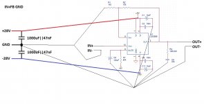
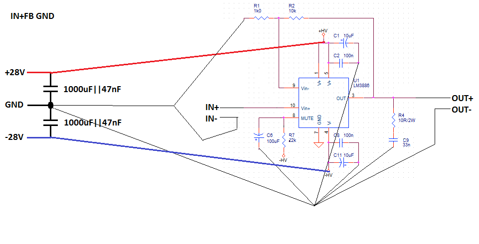
OK, let's take Tom's LM3886 P2P arrangement that measured lowest THD, the one he called IN+FB GND, if he's alright with that?
There is one important thing that is missing from that arrangement: the passive input parts, particularly those that link to ground. An input load resistor and a low pass RF filter.
The idea of separating the grounds in two blocks, low and high impedance, sounds interesting. The question is to identify which ground belongs where.
To get some help I went to have a look at how to use a single supply with a dual-supply IC. To my surprise, all grounds have the same symbol. Which means many people are following that and having higher THD.
Another recommendation I found is using ground (not specified which) traces in between parallel traces to avoid capacitance issues. I wonder which should be the ground trace minimum width in order to prevent that.
But I wonder how you do to identify reference grounds. NFB, which I thought went to reference, goes to mid-point between power and then to star.
Attachments
Last edited:
- Status
- This old topic is closed. If you want to reopen this topic, contact a moderator using the "Report Post" button.
- Home
- Amplifiers
- Chip Amps
- star ground vs. ground plane