It is very difficult to show layout and trace length in a single schematic. You just need to imagine that loops and trace length are minimal. Just look at where each trace connects.
If you only want to see the ground layout only, it may be better to represent the ground as a single line with the returns connecting along that line.
If you only want to see the ground layout only, it may be better to represent the ground as a single line with the returns connecting along that line.
Can I describe a better way?
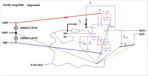
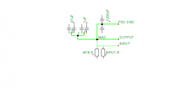
Connect C2 to C8 using a VERY SHORT route. Label this A, HF decoupling ground
Connect C1 to C11 using a SHORT route. Label this B, MF decoupling ground.
Connect A to B Label this SHORT link C
Locate C close to pin3 of the chipamp.
Connect C9 to A or C.
All the preceding capacitors pass High Frequency currents and to do this effectively the impedance must be low. Keep all the preceding trace and leadout lengths VERY SHORT.
Connect OUT- to C This long wire twisted with speaker OUT+ becomes the Main Audio Ground. MAG can be anywhere along this link, but you must choose ONE POINT.
Connect Power Zero Volts to MAG.
Connect Pin7 to MAG.
Connect C6 to MAG.
Connect IN- via a 2r to 20r (HBRR) to MAG.
The RED, BLUE and Power Zero Volts must arrive via a twisted triplet at the MAG and then the +HV and -HV should be located VERY close by.
The input pair must be a close coupled twisted pair or a coaxial. All the way till it reaches Pin10 and the Rin.
The loop area of Rin to the +IN line must be VERY SMALL.
R1 from Pin9 to -IN must be very close to +IN Line to keep loop area VERY SMALL.
R10 must pass across the chipamp package from Pin3 to Pin9 to keep the loop area VERY SMALL relative to the current flows inside the chipamp package. And one end of R10 should connect to NEAR pin9.
Last edited:
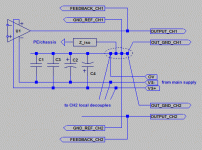
I would just connect 2x1000uF,C1,C2,C8 and C11 to the power ground plane. The smallest caps near to the output return (located near pin3) and LM3886 power pins. Connect PSU to the 1000uF caps.
This layout keeps the capacitor charging currents out of the feedback, input and output grounds.
This layout keeps the capacitor charging currents out of the feedback, input and output grounds.
Attachments
Last edited:
I would just connect 2x1000uF,C1,C2,C8 and C11 to the power ground plane. The smallest caps near to the output return (located near pin3) and LM3886 power pins. Connect PSU to the 1000uF caps.
This layout keeps the capacitor charging currents out of the feedback, input and output grounds.
Wouldn't that increase THD?
One of the things that increases THD is when you place capacitor charging currents in the feedback loop. These currents produce a voltage which is then added to the negative input.
Have a go at analysing the currents in the ground plane of the layout in #64. Remember these amps run in class AB.
Have a go at analysing the currents in the ground plane of the layout in #64. Remember these amps run in class AB.
One of the things that increases THD is when you place capacitor charging currents in the feedback loop. These currents produce a voltage which is then added to the negative input.
The current between the power supply common and speaker common also needs to be kept out of the feedback loop.
No, the speaker connects to the same end of the power supply. In essence, your earlier diagram was correct except that the low-current grounds were connected to a point in the path between the PS common and speaker return.
See attached. The inductance between all the return paths is important, as well as the actual direction of currents. R3/R2 are simplified feedback arrangement.
See attached. The inductance between all the return paths is important, as well as the actual direction of currents. R3/R2 are simplified feedback arrangement.
Attachments
On the speaker output side (to the left of the output return).
The single cap is a simplification of a power supply, the MF/HF caps you probably refer to (decoupling caps?) would be part of this system. In fact they would be on the PCB with a very low-inductance connection to the speaker return.
The single cap is a simplification of a power supply, the MF/HF caps you probably refer to (decoupling caps?) would be part of this system. In fact they would be on the PCB with a very low-inductance connection to the speaker return.
note that post64 is almost identical to this latest post73. i.e. both meet my suggestions in post62
The only part missing is the amplifier Output Zobel.
Once that is added all these should operate equally well
Post69 is different. The output has been taken to a remote PSU. This will increase the impedance as seen by high frequencies.
It may also result in a bigger loop area between speaker flow and return. A bigger loop area will result in more emi.
Firstly there is no such signal as GROUND, think of it as the return current path, work out what you are doing and control the currents... As said many times previous it is rare when I do a board that doesn't have a ground plane (or more often a few) for both digital and analogue (most boards are a mixture of both these days). That doesn't mean I cant control the currents, I do because I think about them and do the layout accordingly and if required will control the flow of high current return paths so they don't interfere with low current paths.
The spindly spiders grounds are silly and can be improved on, but even though many don't know enough to do ground planes they can get over complicated by splitting this up and that up... keep it simple.
This obsession with star spindly legged star ground seems to be only in the DIY audio arena, don't see it in professional audio, instrumentation or any other field of electronics.
As you pointed out there is no "star" nor "plane". It is all a matter of how/where currents flow and how these currents influence reference points. That holds anyway. In fact sometimes when you painting you boards with planes it's necessary to look how the large currents flow (along the lowest impedance) and you will end up with something like a "hidden" star layout.This obsession with star spindly legged star ground seems to be only in the DIY audio arena, don't see it in professional audio, instrumentation or any other field of electronics.
Apart from crosstalk due to trace impedances, you have also magnetic and capacitive crosstalk to take care of: I.e. putting the large air cored output inductor near the input pins of a LM3886 is basically not a good idea without carefully examining crosstalk effects.
That's how I do it (both for audio and measurement amplifiers and such) and it works out every time.
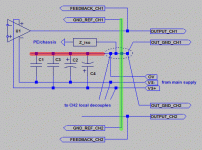
Note the exact sequence on GND nodes in the marked area.
There still is a small local emitting and receiving loop for the output current but that is *inside* the feeback loop so it is not worthwile to minimize it. High freq feedback may be needed to be taken locally right at the chip output when the distances get too large.
Attachments
Apparently that hard-wired comparison was missing something: how you convert that into power and reference planes. And if that improves in THD over the wired layouts.
I mean how do currents flow in a ground plane and how do they stay separate and do not interfere with each other, as on a star ground arrangement?
I mean how do currents flow in a ground plane and how do they stay separate and do not interfere with each other, as on a star ground arrangement?
You keep the currents apart by, well, keeping them apart.
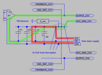
See below, red is the power GND plane, green is the reference GND plane. Also note they are drawn to be a) separated by a significant distance and b) perpendicular to each other. Also note that high current signal cross low current lines with a right angle. This all helps to avoid parasitic inductive coupling to the reference GND.
See below, red is the power GND plane, green is the reference GND plane. Also note they are drawn to be a) separated by a significant distance and b) perpendicular to each other. Also note that high current signal cross low current lines with a right angle. This all helps to avoid parasitic inductive coupling to the reference GND.
Attachments
Next picture: the output current loop (green) and the supply recharge current loop (red). At very low frequencies the output loop extends through the main supply, of course.
All of those currents don't pollute the reference GND.
All of those currents don't pollute the reference GND.
Attachments
- Status
- This old topic is closed. If you want to reopen this topic, contact a moderator using the "Report Post" button.
- Home
- Amplifiers
- Chip Amps
- star ground vs. ground plane