Jaka,
I wonder if your not just observing a probe measurement error due to differences between ground loop return paths?
I guess your scope probe is grounded so you will have an inherently low inductance ground path between the Lower FET D&S, but during the High-side switch, the probes “ground return signal” will have to travel via a much longer return path though the positive supply decoupling to ground – with the associated larger inductances.
I hope you can understand what I’m trying to say… sorry for my poor description.
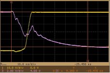
The scope shot below shows Ton, Yellow is OP @ 10V Div, Purple is Gate drive @ 2V Div – notice the effects of Cdg on gate drive
No form of snubbing or clamping has been used Siliconix’s SUD10P06 & SUD15N06
I wonder if your not just observing a probe measurement error due to differences between ground loop return paths?
I guess your scope probe is grounded so you will have an inherently low inductance ground path between the Lower FET D&S, but during the High-side switch, the probes “ground return signal” will have to travel via a much longer return path though the positive supply decoupling to ground – with the associated larger inductances.
I hope you can understand what I’m trying to say… sorry for my poor description.
The scope shot below shows Ton, Yellow is OP @ 10V Div, Purple is Gate drive @ 2V Div – notice the effects of Cdg on gate drive
No form of snubbing or clamping has been used Siliconix’s SUD10P06 & SUD15N06
Attachments
Precisely... Web boards are nice but it's such a typing affair.phase_accurate said:Bruno, we are all ears !!!
Gate driver. Not comparator. Someone forbid people will try driving top and bottom fets with separate comparators.phase_accurate said:There would be solutions to this with cheaper additional circuitry than a 2nd comparator.
But yes, we've done a circuit that can properly mute a pn pair without adding a second driver.

Hi Bruno,
Due to the nature of the OPS EC loop, its irrelevant if the modulator is analogue or digital, it just needs a “PWM” reference signal. As I could not design a digital modulator to save my life, I use off-the-shelf digital modulator – or discrete analogue PWM designs.
With the analogue modulator I achieve less then 0.00005% THD @ 100W 1KHz 8R, 500KHz PWM – in fact limited by the 5534 driving the modulator (Guys - this is development; I would not use a 5534 for listening tests). The 5534 are happy to perform while under the influence of 500KHz carrier components, although it still is the limiting factor - devices like AD797 fall apart in the presents of RF – like me in the presents of beauty.
The advantage of the Digital PWM reference node is the minimal analogue components in the signal path – but I state again that my LP system simply blows away any digital system I’ve heard.
Its been 2 years since I last listen to any of my own digital amp designs – I’m currently building a new PCB which should be complete next week – time not to be afraid of failure (more then 10 years R&D) and Listen!…. how do I already know that the LP / OTL / ESL will win hands down
Parts per billion......
Hi Jon,
Guess this must be like you giving birth, having had the longest gestation period imaginable.......
Its quite refreashing to find a designer who doesnt automatically think that what they have created will be the best thing since sliced bread.
There are some (not those of you who have posted on this thread i might add) who go to great lengths to tell everyone who will listen how great their designs are, deride all others - then fail to support their claims with any meaningful information.....
Back to the amp.....
I am sure it will cut the mustard John....keep us posted.
P.S. What will Bruce Candy and the rest of the Halcro boys do now - as they have 'the only amplifier in the world to challenge the theoretical limit' with 'Unprecedented harmonic distortion levels of less than 1000 parts per billion'.
0.00005% THD i recko thats about 500 parts per bn....
Cheers
Sheriff
Thd
Hi JohnW,
I'm very impressed by the level of discussion between you experts, really. I wonder if I could hear 0.00005% of THD, especially at 100W or more. But I understand the necessity to keep all possible errors in the signal chain as low as possible.
Two little questions:
How does this quite low distortion level match with the datasheet statements (TI slos070B)? Is it a matter of the measurement equipment abilities?
What do you mean with the superior quality of the sound, coming from your turntable? If I remember right, you(?) stated some time ago, that anything, affecting sonic performance should be measurable (at least with the appropriate equipment). Is it possible, that you learned to love your components?
No offence, I take my hat off to you, I can only dream of this knowledge. I whish you a succesful test of the digital amp!
Best regards, Timo
edited:
The THD figure belongs to the TI's NE5534.
Attachments
Hi John,
your explanation is perfectly valid. I recall I had the same noise on the 12V supply rail, so my problem was mainly inadequate decoupling. Next time I wil try to look at the waveform with ground lead attached to +12V.
So this leads me to another topic. Does anybody know good 100V electrolytics for Class D decoupling. For this power supply I used 1000uF/16V ZL series Rubycons or 100uF/20V SA series Oscons, paralleled with 220nF 1210 X7R SMD ceramics. I must say that there was not any discernible difference between Rubycons and Oscons, and also ceramics did not make any visible difference. Rubycons and Oscons are only available up to 35V. Next range that I use are are 450V/10000uF screw terminal ones, but they are not (yet) suitable for class D.
Best regards,
Jaka Racman
While I can’t comment first hand of the pain during delivery, I can say that while offering as much support as I could to my children’s Mother – it was always the stitches afterwards that got me – but then I’m sure that’s more information then is really required here.
I’ve designed more then my fair share of products to know that: -
1. You can never be sure of anything when it comes to audio
2. THD and dynamic range measurements have very little bearing on sound quality
The limiting performance factor in my EC OPS design is not the amount of correction available but the quality of the PWM reference node – and the isolation between the reference and the FB node. At 1KHz, I get about 110 - 120dB isolation – this determines the FB correction limit.
Standard types work best.Jaka Racman said:Does anybody know good 100V electrolytics for Class D decoupling.
Elcaps have a small series inductance that will resonate with the ceramic local decoupling cap, producing an easily visible resonance of a few MHz. The cap's ESR will help to damp this resonance. Using a low ESR type will thus worsen the effect.
I've yet to hear a good sounding low ESR cap anyway.
A good way of getting rid of this resonance is adding a medium sized elcap (between 10uF and 100uF) right across the ceramic. Again, standard types.
JohnW said:The limiting performance factor in my EC OPS design is not the amount of correction available but the quality of the PWM reference node – and the isolation between the reference and the FB node. At 1KHz, I get about 110 - 120dB isolation – this determines the FB correction limit.
I can't help thinking of such statements mostly as crafty circumlocution.
My guess is that a pair of so8 fets can get you an uncorrected timing error of 500ps (that's what I get from such a setup anyway).
At full output and 500kHz that translates into about 0.01%.
If this is a 3rd harmonic and in closed loop you get 0.00005% loop gain must be 200 at 3kHz.
A second order loop will happily do that and more.
So we see loop theory is sufficient to explain the result. That the input signal be PWM is therefore not instrumental to the outcome.
Timo,
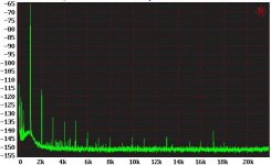
I guess TI was having bad day when they measured there NE5534, below’s an FFT I perform just for you - of a LM5534 @ 2Vrms 1KHz, THD 0.00017 - Excluding second harmonic THD 0.000033%. Due to the balanced nature of my modulator designs, even order distortion products are reject to a large degree.
Yes, I stand by my statement that anything that effects “sonics” is measurable – but its how & what we measure – and then how we translate these measurements into quantative results. E.g. what does 1% THD really mean? 1% second or 1% 10th… 1% second I can live with, however 1% 10th – and the units going to learn to fly….
John
LM5534 @ 2Vrms 1KHz 1K load
I guess TI was having bad day when they measured there NE5534, below’s an FFT I perform just for you
- of a LM5534 @ 2Vrms 1KHz, THD 0.00017 - Excluding second harmonic THD 0.000033%. Due to the balanced nature of my modulator designs, even order distortion products are reject to a large degree.Yes, I stand by my statement that anything that effects “sonics” is measurable – but its how & what we measure – and then how we translate these measurements into quantative results. E.g. what does 1% THD really mean? 1% second or 1% 10th… 1% second I can live with, however 1% 10th – and the units going to learn to fly….
John
LM5534 @ 2Vrms 1KHz 1K load
Attachments
Dear John,
you will hardly find better AM receiver than NE5534 . I was checking several opamps in the position of RIAA preamp, and 5534 was the winner (together with 1458) as an AM receiver. But in terms of sonic quality OPA2134 was definitely better.
Look forward to seeing you soon with your new amp,
Pavel
you will hardly find better AM receiver than NE5534
. I was checking several opamps in the position of RIAA preamp, and 5534 was the winner (together with 1458) as an AM receiver. But in terms of sonic quality OPA2134 was definitely better.Look forward to seeing you soon with your new amp,
Pavel
Pls. excuse my ignorance I haven’t that faintest idea what “circumlocution” means – passed it though MSWORD grammar – but no luck…
Anyway, in my experience the greatest distortion at higher power levels is the result of RdsOn and PSU issues – The only recorded open-loop results I have is with the ZETEX 8100 operating @ 1MHz – 1KHz 126W 8R 0.25% which would need about 80dB to reduce to say 0.000025% - but the ZXCW8100 modulator on its own produces 0.039% at 0dB 1MHz HPWM – yes its V poor – and especially considering its 1MHz switching rate!
So while I will have more then enough loop gain at say 3KHz, the story is not so clear at 20KHz (for IMD) – unless I add Zeros to the FB loop… which can be done but…
So I standby my statement that from experience the quality of the PWM reference node / modulator is important - and currently the limiting factor.
You mentioned that I could try your FPGA modulator design – which would be very interesting: -
1. Which FPGA device - XILINX Spartan type or Actel types – pls. not BGA!
2. Input MCLK 2048fs?
3. PWM fs 384KHz / 768KHz?
4. Input format?
If that's the case you've got the kind of timing errors I was mentioning. Otherwise timing dominates.JohnW said:Anyway, in my experience the greatest distortion at higher power levels is the result of RdsOn and PSU issues.
Zetex... c'mon you're joking...
Anyhow fyi THD = 0.4*td*fsw where td is peak to peak timing error. It's only a rule of thumb, because the actual shape of the timing error vs current is the main determining factor.
At 20kHz a second order loop still pulls 40dB. 80dB+40dB=120dB.JohnW said:So while I will have more then enough loop gain at say 3KHz, the story is not so clear at 20KHz (for IMD)
So I standby my statement that from experience the quality of the PWM reference node / modulator is important - and currently the limiting factor.
Unless you are predicting the error, the system must be mathematically reformable into a classic control system (with or without deliberate or accidental nonlinear elements). I may or may not succeed in correctly guessing the nature of the equivalent loop function, but mathematical truths are rather much a solid affair.
And of course the PWM reference node is important. That's what you're telling the amp it should do. Same for the DAC in a normal DAC+Amp combination.
Here's a suggestion on how to work the reference node problem. You have a power stage with correction that responds to PWM. Well, put it inside a normal 1st order loop. The same kind you were probably using in the analogue test modulator. That reduces the requirement placed on the logic buffer.
1st order loops are inherently linear (higher order loops are inherently non-linear due to the presence of non-rectilinear waveforms as produced by the higher order integrators).
The latter happens to explain why a loop having a PWM input signal is potentially more effective. Presuming a sufficiently low delay, the output of the summing node has nearly no carrier components compared to the case where the feedback is PWM but the input signal isn't. This allows the construction of higher order PWM control loops without adversely affecting linearity because there is very little HF to do so.
(Actually I was hoping to hear the above from you, hence my challenges. Maybe you could make clear which things you are willing to divulge and which things not - saves the effort of guessing when it makes sense to prod and when not)
Actual sharing of the design has to wait until the patent application is filed - which shouldn't be that long.JohnW said:You mentioned that I could try your FPGA modulator design – which would be very interesting: -
1. Which FPGA device - XILINX Spartan type or Actel types – pls. not BGA!
2. Input MCLK 2048fs?
3. PWM fs 384KHz / 768KHz?
4. Input format?
We've always used altera acex types but 2048fs is just out of reach for them. It's the only vendor we have the mapping tools for.
PWM runs at whichever speed you want it to run at. For "real" open-loop designs it's kept low (ie. 8fs) to keep power stage thd low. It isn't awfully complicated to change that.
Input is normally the kind of format put out by DF1706 type chips.
Cheers,
Bruno
Bruno,
No kidding about the Zetex, THD is not the only problem – the modulator generates large amounts of noise floor modulation and non-harmonic spurie at higher modulation levels – although in its 2MHz HPWM mode its better behaved
My EC power stage can operate at 2MHz but idle current switching losses for a full bridge are in the order of 120mA at 55V.
When I talk about the PWM reference node, I’m talking about two issues.
1. The basic modulator performance in the digital domain
2. Reference Latch / Buffer that drives the EC circuit - which then forms the “PWM” reference node
I had considered using a first order correct loop for the reference node – but not for the reasons you mentioned.
Unless I misunderstood your description, there’s little point in implementing a first order FB loop around the reference node / OPS as the basic error is in generating the actual reference node signal. A FB loop afterwards will not help as there’s no point of applying FB correction without having an accurate reference – and if I had and accurate reference in the first place, I would not need the 1st order FB loop!
I could not think of a way to generate the low level PWM reference node without incurring the even-order distortions caused by non-symmetrical gain of the Pch (high) / Nch (Low) PWM buffer (due to differences of there RdsOn values). With typical H /L difference of say 2 Ohms which when driving a typical 1.5K EC input load would result in even-order distortion products at –57dB. Now while this distortion would be ultimately rejected by the balanced nature of the HBridge – I strongly disagree with poor single-ended performance – its just bad engineering…
My solution was to use a first order integrator, with symmetrical inputs from the modulator to generate the reference node thereby cancelling even order components. But in the end, (rightly or wrongly) I felt that the reference node was no longer digital, and unknown “analogue” type distortion components could be introduced by the integrator – especially one that relied upon common mode rejection of its inputs.
Of course, even stating that the PWM reference node is “Digital” is misleading as it’s ultimately referenced to an ultra low noise PSU linear regulator based around a good old 5534 and not to forget the Clock phase noise! So, at the end of the day there’s always an analogue FB loop around the reference node in one form or another.
So I used simple brute force and reduced the Gain error ratio – the result is that common mode distortion across the bridge is now below –100dB at FS.
The feedback thing was in case the input is analogue. As you're basically saying, you're excercising your capabilities as a DAC designer in terms of the reference pwm node. The analog loop would retain the quoted advantage of having the main correction operating with pwm both on feedback and input side, whereas the actual "amplifier" input can be a normal analogue signal - possibly from a dac having better THD performance than what you could do there.
So much for the principal argument. I design DACs with logic buffers as well and find no "DAC" chips can outperform these designs (THD-wise, will refrain from bragging about the sound), so total performance of your system can indeed be better than a perfect analogue amp plus any other dac (disregarding the post filter issue)
In practice this corroborates your concept of best system performance. This is quite interesting, considering that the actual real digital amplifiers (tact etc) are the path to the worst system performance...
I would not underestimate the sonic advantages of post-filter feedback though. I've also toyed with simply moving up the cutoff frequency and never got anywhere near the sound quality of total feedback. If you're looking for the airy dryness of analogue, this is it. Even then the output cap/coil leave a noticeable signature on the sound, but it's definitely less than what a filter without feedback does.
The fact that feedback after the output filter immediately creates a higher-order loop is a problem, because the linearity problem creates more distortion (open-loop-wise) than a tightly designed power stage. In that light, pulling the trick of placing a high order pwm i/o loop in a UcD loop would not give as low THD as a first order loop without filter correction. The question shall be whether loop distortion (purely 3rd) of -90dB is high enough to mar the listening experience compared to lower THD but no filter feedback.
Concerning your analogue reference system I'd like to note that no low-voltage amplifier + stepup transformer can ever sound as good as a HV amplifier directly driving the electrostats. You can make the perfect wire-with-gain but the stepup will blow it for you. Putting feedback around the transformer should work but places us firmly back into fully analogue terrain.
Cheers,
Bruno
PS: What I meant with Zetex and kidding is: when they visited me and showed the documentation I could not suppress a laugh. Open loop analogue. The worst of two worlds. So I was surprised to find that you actually did bother to touch their hardware.
Jan-Peter (or Bruno, if not quite busy),
yesterday i had try to build UcD with second loop feedback, and THD have same tend to grow with frequency, of course.
By the MC7 simulations i expected 0.002% at 1khz, and 0.004% at 10khz,
but real THD was 0.016%@1khz and 0.07%@10khz (at 500hz about 0.007% etc to the limit of my audigy- 0.002%..what can i do if haven't AP? AP sys2 is ok, AP sys1-sob, without AP -$40audigy.
Unfortunately only 4 hours of the weekend left for this experiment, and only TL084 (SO14) was available at moment (also, for this new PCB version, i'm still haven't listening/measurement), therefore i'm sure that's very preliminary result. However..
Mostly interesting that sound of the my old AB and modified UcD now exactly same,
and no more transparency & high resolution, just a blured [feedback?] sound.
My reference listener (my son after listening say same...
Jan-Peter, what about sound of your UcD+2nd loop?
PS (just a lyric): Yeah, 5E-5 THD it is something..IMHO it's HUGE work!Sometimes i ask myself: why people ready to spend so much resource for audio (entertainments generally), but not for fundamental or medical research?
yesterday i had try to build UcD with second loop feedback, and THD have same tend to grow with frequency, of course.
By the MC7 simulations i expected 0.002% at 1khz, and 0.004% at 10khz,
but real THD was 0.016%@1khz and 0.07%@10khz (at 500hz about 0.007% etc to the limit of my audigy- 0.002%..what can i do if haven't AP? AP sys2 is ok, AP sys1-sob, without AP -$40audigy
.Unfortunately only 4 hours of the weekend left for this experiment, and only TL084 (SO14) was available at moment (also, for this new PCB version, i'm still haven't listening/measurement), therefore i'm sure that's very preliminary result. However..
Mostly interesting that sound of the my old AB and modified UcD now exactly same,
and no more transparency & high resolution, just a blured [feedback?] sound.
My reference listener (my son
after listening say same...Jan-Peter, what about sound of your UcD+2nd loop?
PS (just a lyric): Yeah, 5E-5 THD it is something..IMHO it's HUGE work!Sometimes i ask myself: why people ready to spend so much resource for audio (entertainments generally), but not for fundamental or medical research?
Ivan,
Thanks you show us your measurings! This is not bad at all.
To tell you the truth, nobody didn't yet listen to the UcD with an active integrator loop. However I have send Bruno recent two UcD modulators with an active integrator feedbackloop, for acoustical testing. So we have to wait for his comment on the sound of this version of the UcD..........
Besides this, Bruno did calculated the new values for the loopfeedback! Within a few days I can show probably some new measurements with hopefully even lower THD's.
Our mainproducts are subwooferamplifiers, with this active integratorloop we can now create Class-D amplifiers with an outputimpedance of <0.001 Ohm............
Did you do a listening test with your UcD and the other Class-D amps what you have made? (Soda?)
Can you show us also your implementation of the UcD?
Regards,
Jan-Peter
www.hypex.nl
- Home
- Amplifiers
- Class D
- Which chip and whatever happened to Mueta and UCD?