Hi Sheriff,
I have one of Pauls very first system. This system is just as bad as the AP1 for RF IMD and DR.
My early version (1st?) uses the CS5327 on a National Instruments PC card, maybe his current units have pre-filtering in the external boxs.
I used to use it for Jitter testing, untill I discovered that most Jitter "components" below 100pS where due to ADC IMD products, and not Phase noise. Adding a 20KHz brickwall to the cards input removed about 100pS of Jitter!
John
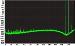
JohnW said:Below is an FFT of a TRUE digital amplifier, 118W 8Ohms 997Hz THD 0.0003% modulator and clock limited. Awtd dynamic range 114.5dB – again modulator limited.
118W 8Ohms 997Hz THD 0.0003% DR 114.5dB
How true is "true"?
There's a dane selling a "digital amplifier" that employs a secondary analogue feedback loop (pedec), which implies the loop considers the buffered "digital" signal as its analogue reference.
"true digital" should mean open loop - no correction of switch timing whatsoever because that would be a non time-discrete action (ie. analogue).
Waiting curiously, because the results surely look excellent (regardless of whether analogue processing was involved or not btw). THD vs frequency plots would be very welcome.
Re: AP and production
If you tie a 1uF cap straight to the output without a speaker cable (=series impedance) and subsequently overdrive it you can make it go unstable.
This situation is fairly rare though. You can rest pretty assured the amp is left quite cold by the load.
Sheriff said:On a different topic to THD, Bruno mentions in an earlier post that UcD with the second integrator loop is unconditionally stable.
From this statement can i assume that it will drive any capacitive or inductive load, and give essentially loudspeaker independant performance?
If you tie a 1uF cap straight to the output without a speaker cable (=series impedance) and subsequently overdrive it you can make it go unstable.
This situation is fairly rare though. You can rest pretty assured the amp is left quite cold by the load.
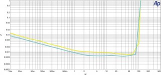
Hi to All,
Some measurements at R&D when I am playing with an improvement on the UcD......
Measurement is with 4 Ohm and 8 Ohm load and by 1kHz.
Green is 8 Ohm and yellow is 4 Ohm.
Regards,
Jan-Peter
www.hypex.nl
Some measurements at R&D when I am playing with an improvement on the UcD......
Measurement is with 4 Ohm and 8 Ohm load and by 1kHz.
Green is 8 Ohm and yellow is 4 Ohm.
Regards,
Jan-Peter
www.hypex.nl
Attachments
I don’t perform THD vs. Frequency sweeps as nothing annoys me more then seeing manufactures publishing THD sweeps to 20KHz with the AES17 filters enabled and the AP in 22KHz analyser Mode!!!
I perform 7.2KHz THD test (2nd & 3rd in audio band), but once again, the results are limited by the front-end reference modulator.
I do have 19KHz and 20KHz IMD results at 120W 8R – but these are limited by the R&S UPD05 having a near death experience. For dual tone IMD tests I cannot use the UPD’s “single frequency” notch filter, so what you see is the true resolution of the UPD’s ADC (i.e. without the benefit of the ~30dB dynamic range gain by using the internal notch filter) – the components you see at lower frequencies are the result of this near death encounter.
Despite this, the 3rd order IMD components of –115dB @ 120W 8ohms put most – if not all amplifiers to shame – the real level of these components could in reality be lower – who knows how much is due to the digitising ADC – and don’t forget that this is a total “replay” system result – ignoring speakers (i.e. no DAC or Pre-amp distortions to add).
In addition, although better then the AP1, the UPD has a real problem with “RF IMD”, unfortunately the UPD internal ADC’s sample at 48KHz, which “beat” with components of the 384KHz PWMFs (8fs).
The Amplifier is “TRUE” digital in the sense that the modulator is digital, continues time correction is applied around the OPS – which is not PEDEC.
John
19KHz and 20KHz IMD results at 120W 8R – once again results are UPD / modulator limited. They are identical to the modulators PWM reference node.
Attachments
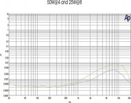
Again a measurement frequentie against THD in 4 and 8 Ohm with an outputvoltage of 13,5Vrms.
This are some mesaurements to see how shocking low a THD can be with a Class-D amplifier. Please notice this are really pre R&D measurements, where we only used some standard values for the Class-D modulator.......
I am really wondering how good will it be when the right components values are known ;-)
Regards,
Jan-Peter
www.hypex.nl
 I REST MY CASE
 I don’t perform THD vs. Frequency sweeps as nothing annoys me more then seeing manufactures publishing THD sweeps to 20KHz with the AES17 filters enabled and the AP in 22KHz analyser Mode!!!
If look at the above THD plot, you will notice the distortion drops off at higher frequencies, as increasingly less harmonics are in the measurement bandwidth - basically a meaningless graph above ~ 10KHz as even the second harmonic is now outside the 20Khz measurement bandwidth!
Pls. note that this is in no way a criticism of Jan-Peter, as 99% of manufactures perform & publish the same test!
But never the less, a very good result for such a simple design
") Bruno - how about calculating those optimised integrator component values for Jan?
Bruno - how about calculating those optimised integrator component values for Jan?John,
Ofcourse I agree with you. But measurement is also intepretating the graphs! You can increase the measurement bandwith of the AP, but the disadvantage will be the increasement of the noise.
So, In this case you woudn't see how good the amp performs at lower frequencies.
In a way you should measure with different bandwith settings of the AP.....
You have all the tools, can you show us your freq to thd graph?
BTW, I am VERY satisfied with AP Sys2 for R&D, we use the ATS2 for production (much cheaper).
Regards,
Jan-Peter
Poor relative...
Hi John,
Looks like i am a pretty poor relative only having a AP sys 1 (sob).
The latest of Pauls stuff is really geared toward multichannel testing, so i guess (without speaking to him), that he has not had that many requests from manufacturers re class D apps. (well certainly not in the UK).
You have obviously spent a long time developing your amplifier, are you willing to share a little more about it?
Cheers
Sheriff
The AP2's internal AD can be run at up to 108kHz for the high-resolution mode (the high speed AD has aliasing problems, just like the ole AP1). If you use the harmonic analyser (digital analyser panel) you can measure THD without noise with harmonics up to 50kHz. This allows one to have a wider-band measurement (the AD's distortion may become an issue).
One should wonder if the harmonics over 20kHz matter though. After all they *are* outside the audio band. Inband IM products associated with higher audio frequencies obviously do matter.
While it would be intellectually more correct to stop the THD vs F plot at 7kHz (or 10kHz in my case) I'm sure you'd be deluged by mails from "nonunderstanding interested parties" (marketing people) asking why the graph stops there. Hence the habit.
But John, I won't think bad of you if your THD vs F graph stops at 7kHz.
Concerning simplicity... Does your amp have any provision to insure the frequency response stays flat? TacT went all the way to telling users they had to buy the room response equaliser which would then also automatically include the amp's response deviation.
I find it quite easy to get super-low THDs if I don't have to worry about the output filter (or EMI. At least my amps don't upset AP's. Or tuners in the same box), but then one should wonder whether several dB's of unpredictable deviation from flatness isn't going to produce more colouration than the distortion does.
That consideration of course does not detract from the fact that -110dB on a single-phase power stage is "quite" an achievement.
Btw if you have modulator THD problems I can roll you a better one. The current version produces -150dB THD at maximum output. Single-edge. 3000 ASIC gates (FPGA gate count is about 15k). No DSP. If it is true that your current THD figure is largely that of the modulator it may be worthwhile.
The biggest weakness of my topology is the sensitivity to speaker loading effects, although the corner frequency point can be set at 100KHz (with a 768KHz PWMFs), and still achieve good EMC performance. With a 100KHz FC - the effects of speaker loading are minimal (less then say 0.5dB) – my conventional DAC designs for Cambridge audio and Pink Triangle had greater roll-off then this at 20KHz.
Although this might seem an odd statement, frequency response does not tell us much about sound quality – the brain seems to compensate very quickly to irregularities in frequency response. Most speaker systems have very lumpy frequency responses in real listening environments, typically +/- 5dB across the band from say 50Hz to 20KHz – but add less then 0.005% crossover distortion, or non harmonic spurie -140dB down - on the noise floor and things get very grim – very quickly
The higher PWM frequency also allows greater dynamic range from the modulator & better AM tuner compatibility.
Sure, the ability to take feedback after the LPF is a preferred solution (as with your designs), but then this FB is truly analogue in nature (which I’m not saying is a bad thing). Time will tell if the benefits of a “true” digital amplifier outweigh its disadvantages – or if combining a DAC and an “analogue” Class D is a better solution. Either way both of these “integrated” solutions promise fair greater sonic advantages over current DAC / Pre / Power solutions.
On the AP2 subject, my lab is already so cluttered, trying to find space to balance a laptop and its “Mouse” to use the drop down menus to operate the AP, just does not seem as easy as pressing single function hardware buttons on the UPD. The FFT feature is slow and clumsy on the AP2 C+ – but its ultimately higher performance (and the AP’s have time aligned averaging) and are the industry standard. I have both, but I doubt the AP’s have been powered up for more then 24 hours over the past couple of years – and can I set the 200 or so dip switch’s correctly to get I2S output – not yet
The output stages are full bridge – AD or BD does not matter.
I might take you up on your offer of the FPGA, although I’m more interested in Stop-band rejection (but I’m guessing that with only a 15K gate count that the “digital filter” is off chip), in-band noise floor / dynamic range, and the amount of data truncation / rounding between stages (width of internal data paths)…. the fact that you have achieved a THD of 150dB, I guess you have a very good PWM linarizer design to say the least!
Currently, digital modulator manufactures consider the ultimate limiting factor to be the OPS, which is not the case with my OPS topology. Also, the modulators are being designed for budget DVD solutions, where audio performance is not an issue. Within the next few years, the modulator sections themselves will be integrated within the DVD decoder chipset, leaving the hopes for high-end digital amplifiers stranded.
Sheriff, Email me, and I can send you some external filter designs for your AP1.
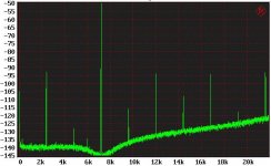
The PCB that I used for the prototype results has long since been butchered for some worthy cause, but found a 7.2KHz 127W 8R FFT. The graph is not a pretty sight due to the very poor stop-band rejection of the TAS5015 modulator used in the test (-65dB), the 3rd harmonic component is right on the edge of the Stopband, and as can be seen, really upsets the digital filter in the TAS 5015. For the record, there’s was almost no difference (spurie pattern within 1dB) between the Modulator PWM reference node and output – so again the modulator is the limiting factor.
TAS5015 7.2KHz 127W 8R – non-harmonics are due to the extremely poor Stopband rejection of the TAS5015
Although this might seem an odd statement, frequency response does not tell us much about sound quality – the brain seems to compensate very quickly to irregularities in frequency response. Most speaker systems have very lumpy frequency responses in real listening environments, typically +/- 5dB across the band from say 50Hz to 20KHz – but add less then 0.005% crossover distortion, or non harmonic spurie -140dB down - on the noise floor and things get very grim – very quickly
The higher PWM frequency also allows greater dynamic range from the modulator & better AM tuner compatibility.
Sure, the ability to take feedback after the LPF is a preferred solution (as with your designs), but then this FB is truly analogue in nature (which I’m not saying is a bad thing). Time will tell if the benefits of a “true” digital amplifier outweigh its disadvantages – or if combining a DAC and an “analogue” Class D is a better solution. Either way both of these “integrated” solutions promise fair greater sonic advantages over current DAC / Pre / Power solutions.
On the AP2 subject, my lab is already so cluttered, trying to find space to balance a laptop and its “Mouse” to use the drop down menus to operate the AP, just does not seem as easy as pressing single function hardware buttons on the UPD. The FFT feature is slow and clumsy on the AP2 C+ – but its ultimately higher performance (and the AP’s have time aligned averaging) and are the industry standard. I have both, but I doubt the AP’s have been powered up for more then 24 hours over the past couple of years – and can I set the 200 or so dip switch’s correctly to get I2S output – not yet
The output stages are full bridge – AD or BD does not matter.
I might take you up on your offer of the FPGA, although I’m more interested in Stop-band rejection (but I’m guessing that with only a 15K gate count that the “digital filter” is off chip), in-band noise floor / dynamic range, and the amount of data truncation / rounding between stages (width of internal data paths)…. the fact that you have achieved a THD of 150dB, I guess you have a very good PWM linarizer design to say the least!
Currently, digital modulator manufactures consider the ultimate limiting factor to be the OPS, which is not the case with my OPS topology. Also, the modulators are being designed for budget DVD solutions, where audio performance is not an issue. Within the next few years, the modulator sections themselves will be integrated within the DVD decoder chipset, leaving the hopes for high-end digital amplifiers stranded.
Sheriff, Email me, and I can send you some external filter designs for your AP1.
The PCB that I used for the prototype results has long since been butchered for some worthy cause, but found a 7.2KHz 127W 8R FFT. The graph is not a pretty sight due to the very poor stop-band rejection of the TAS5015 modulator used in the test (-65dB), the 3rd harmonic component is right on the edge of the Stopband, and as can be seen, really upsets the digital filter in the TAS 5015. For the record, there’s was almost no difference (spurie pattern within 1dB) between the Modulator PWM reference node and output – so again the modulator is the limiting factor.
TAS5015 7.2KHz 127W 8R – non-harmonics are due to the extremely poor Stopband rejection of the TAS5015
Attachments
The issue I have with THD vs. Freq plots is what are the curves showing above 10KHz when the AP is set to 22KHz mode and the AES17 filters enabled?
Above 6.6KHz, only the second harmonic is in the measurement bandwidth, and above 10KHz, all harmonics are now out of the measurement bandwidth – so again what are the curves showing above 10KHz? Well for sure it cannot be THD – so its wrong to represent them as such.
It seems that Bruno shares the same love of marketing guys as I, and correctly asks is THD above 10KHz important? However, bare in mind that THD tests are just simple “Static” tests to give us an idea of the systems linearity under dynamic conditions.
I believe that the IMD 19/20KHz to be a better test of system THD with a 22KHz measurement BW – at least the second & third harmonic components are within the measurement BW.
Bruno - Out of interest, do you have any 19/20KHz 100W IMD measurements of UCD?
I have a direct drive (4KV) OTL valve amp driving ESL panels with a turntable as the source – Total system THD I’m guessing will be around 1-2% (if not more), but I’m still waiting for the day I hear a “Digital” system compete in sound quality – this despite spending more then 15 years designing and developing “Digital” products – which is quite a sad statement….
The issue I have with THD vs. Freq plots is what are the curves showing above 10KHz when the AP is set to 22KHz mode and the AES17 filters enabled?
Clearly nothing, admittedly. But sometimes measurements are made with less restrictions. That's why I said that the conditions should be stated.
BTW: Your modulator really seems to behave damn well !!!!!
Regards
Charles
Hi Bruno,
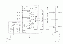
from your description of PPA amplifier it seems that it is roughly similar to the concept of Yamaha Yamaha MX-D1 amplifier. The principle of modulation can be seen in US patent application 2003/0058038 and in attached picture. Although Yamaha uses dedicated chip modulator, I think something like that may also be DIYable in multiphase version?
John,
I remember that you use complementary pair in your output stage. Recently I had to develop a 2V/45A power supply. I used 3 phase synchronous buck converter running from 12V. All FETs were Nchannel SO-8 devices, compact layout and 4 layer PCB. I have noticed the same phenomenon for the second time. I had ringing on top of the low to high transition of the half bridge, that is when upper FET turned on. But the high to low transition was exceptionally clear, no ringing whatsoever. Now I don't know if that has anything to do with the fact that lower FET was operating in ZVS (zero voltage switching) regime, or that it was in common source configuration in contrast to source follower configuration of the upper FET. I had previously used complementary source follower configuration, but I had this 10V 10ns spike and some ringing on both transitions, regardless of supply voltage (from10 to100V). I noticed that Yamaha also uses complementary common source pair and it is said that newest Tripath modules use it also. How clean are your switching waveforms?
Best regards
Jaka Racman
Attachments
Since I've sufficiently argued in writing how bad the idea of a power DAC is, and since John's amplifier is clearly a good amplifier, I shall proceed to argue that John's amplifier is not a power DAC or "true digital amplifier". Of course, if I get one assumption wrong I'll go flat on my face but that's what life is about.
At some point in the amplifier there is a logic buffer that tells the amplifier when it should ideally switch. One correction method would be to check at each edge when the actual transition has occurred and use this knowledge to shift the next transition (of the same polarity) back or forth.
Quite clearly this is not the only thing that's done here. Even for a bone-hard power supply, psu impedance related distortion would still be present.
For a full bridge, psu-related THD = Rpsu/(4*Rload*modulation_index^2)
Thus, the edge correction used also takes account of some power rail modulation. The most effective way is simply integrating the error between of the logic buffer's output and the power stage output, not just at the edges but always, and using the result to correct subsequent edges. The effectiveness of such a system at doing so is for all intents and purposes called loop gain.
I expect this is more or less what John's amplifier does. If not, you can skip the rest of this post.
Suppose one superimposes a small audio signal onto the logic buffer's output, and that the logic output is carrying an unmodulated square wave. The amplifier would effectively try to reproduce this audio signal and remodulate the edges in order to do so.
If it weren't for modulation reserve, the amp would handle a square wave with a superimposed audio signal with equal precision as a square wave having the LF content modulated onto its edges.
So, topologically speaking the logic buffer is the actual DAC, and the following stage is analogue.
Which incidentally is what I've always proposed. Keep the DAC in the small signal domain and use an analogue amp. Roughly synchronising the amplifier's operation to a PWM DAC has no effect on the topological buildup and hence classification of the device, but it does complicate the design for no obvious reasons (except possibly to substantiate a claim of "true digital") and with no objective effect.
So, John, how about coupling your obviously excellent power stage to a non-index-restricted analogue modulator? It would allow you to separately optimise the modulation strategies used in the DAC and the amplifier for yet a better result.
Hi Jaca,
Apparently the MXD1 uses a flash converter followed by a digital pulse width modulator. This is of course an unnecessary complication. The same result is obtained by an analogue PWM circuit.
It is a typically Japanese phenomenon to add circuitry for the sake of "more proprietary technology" without reaping any technical benefit. Usually the results are worse than what the simple solution would have done. Sometimes a large number of extra measures have to be taken in order to counteract the negative effects produced by the added technology.
That said, feeding the control output into an AD and digitally processing that signal for use by the power stage is also done by PPA. There, this is done because the power stage can reproduce a multitude of voltage levels. So, you need to quantise first. The digital processing is necessary in order to keep the currents in the output inductor network (center tapped chokes) around zero.
To answer the P/N mos question, my sodas used p/n mos pairs. This can be beneficial if the gates are coupled directly, because it automatically synchronises switchover. This can significantly reduce energy stored in lead inductances and recovery charges. The latter is somewhat offset by the greather recovery charge of the p parts.
For this reason, quite often you can use much less (if any) snubbering on pn pairs than on nn pairs.
Drawbacks are added complexity to prevent both fets from turning on at power-up and difficulty disabling the output stage. Using two separate drivers would solve these but completely obliterates the advantages of pn pairs.
Also, p mosfets are often a generation behind on their n counterparts. There's a serious risk of designing amps with outdated fet technology.
For these reasons I've moved to nmosses and work on more subtle gate drive tactics. I could talk for hours on how to turn a fet on and off in the most optimal way.
I could talk for hours on how to turn a fet on and off in the most optimal way.
Bruno, we are all ears !!!
Regards
Charles
Drawbacks are added complexity to prevent both fets from turning on at power-up and difficulty disabling the output stage. Using two separate drivers would solve these but completely obliterates the advantages of pn pairs.
There would be solutions to this with cheaper additional circuitry than a 2nd driver.
Regards
Charles
Edit: changed "comparator" for "driver"
- Home
- Amplifiers
- Class D
- Which chip and whatever happened to Mueta and UCD?