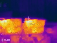
The current source dissipates (10 - 5) * 0.13 = 0.65 watts. Its case rises to 58C which is 33C above ambient air. That means its thermal resistance from case to ambient air (theta_CA) equals (33 / 0.65) = 51C per watt. That's a pretty impressive transistor, since most TO-126 medium power transistors are rated 100C per watt.
{And if there's no load on the regulator output, the shunt device dissipates the same: (5 - 0) * 0.13 = 0.65 watts}
{And if there's no load on the regulator output, the shunt device dissipates the same: (5 - 0) * 0.13 = 0.65 watts}
Last edited:
@Vunce
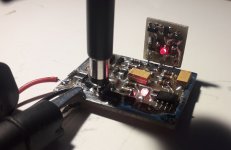
I finished the design, I preferred to put two pads in the case I would like to implement the cascode for the dn2540, so as to be able to experiment with new solutions with a small daughter pcb. I tested the operation for an output voltage of 5v and a current of about 80mA, everything works correctly, as soon as I complete the assembly of the pcb I will start preparing everything to be able to power the dac and see if everything is fine. I am attaching the eagle files if someone might need them.
Ad maiora.
Attachments

- Home
- Amplifiers
- Power Supplies
- Walt Jung shunt Design