")
@grunf
Hi Grunf
I am testing the regulators well before assembling them well and connecting them to various chips, I measured a voltage drop of 1V on R4 and therefore a ccs current of about 200mA, this current is too high for the use I will have to make of it, considering the consumption of the regulator itself which is 25mA and of the gled which is 5mA, we have a consumption of the shunt alone of about 30mA, we must then add the 30mA needed for the power supplies and therefore we are at 60mA, add 10mA for reserve, and we have a total current of 70mA, so how can I calculate the Rset for my current? I can't find my answer.
@Tix88, you have to increase the value of R4 to about 5.6R and try to measure the current again, also with R16 set Vds for the lower mosfet to be half the voltage drop if the DN2540 is the lower mosfet. If the BSP149 was there, it would only need 2V. R10 must be 150R not 200R.
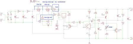
I forgot that Vds Q1+Vds Q2 must be at least 20V for 2xDN2540, in my case only 5V is needed for BSP149 and BSS159.
I forgot that Vds Q1+Vds Q2 must be at least 20V for 2xDN2540, in my case only 5V is needed for BSP149 and BSS159.
Attachments
Last edited:
@grunf
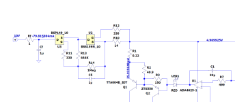
Hi Grunf, the schematic I'm using is this, not the one with the cascode, because it's not quite ready yet, I'll use the components you recommend, for a lower voltage drop. In any case I always have to increase R4 right?
Hi Grunf, the schematic I'm using is this, not the one with the cascode, because it's not quite ready yet, I'll use the components you recommend, for a lower voltage drop. In any case I always have to increase R4 right?
Attachments
@grunf
Hi Grunf, I did some testing, but I probably made a mistake earlier in the measurements. I disconnected the opamp from the circuit, and measured the voltage drop across the r4, until I calculated a current of about 84mA, increasing the resistance up to approximately 15R, I measure across it at 1.3V. I reconnected the opamp and redid the measurements and this is what I measured
R4= 1.32V
Pin3 OPA= 2.48V
Gate dn2540= 4.97V
Drain = 15.83V
Source = 6.30V
VGS= 1.32V
Vout= 4.96V
At this point I think everything is correct
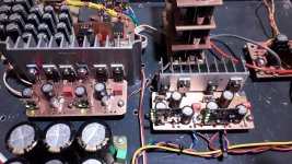
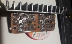
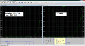
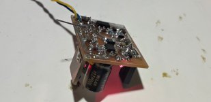
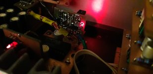
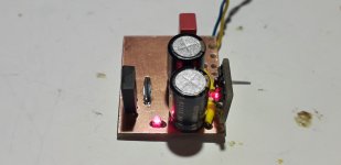
The 500mA version was finally tested yesterday and it was immediately installed in my DAC as a regulator for eight PCM1702s. Output voltage is +/-5V, input +/-19V, mosfets are IXTP08N50D, dissipation on them is ~10W, which is also the total dissipation of the regulator. Output currents are currently set to 420mA for - and 170mA for +. The 2.5V reference is a Walt Jung low noise reference (upgraded GLED431).
As for the results, I have to admit that I'm delighted, so far it's definitely the best regulator that I've made in the last 15 years since I've been working on discrete regulators.
Regardless of the fact that it does not work in the analog domain, but in the digital domain, the difference in sound is very audible. Really great regulator.
Attachments
Last edited:
Hi grunf,@Tix88 , you don't need any jfets, only depletion mosfets, for example, BSP149 and BSS159N are excellent for such small currents, I use them up to 120mA with a maximum of 5V voltage drop across them.
I was wondering if the 5V headroom for two mosfets is enough. Does the rule of Vds > 2*Vgs(off) applies here? BSS159N has about 3.5V Vg(off) which gives at least 7V of Vds, This is already above 5V not mentioning BSP149. Just curious. And impressive work and contribution btw.
Mariusz
Thanks @Tix88 and @mariush
mariush ,a bit about depletion mosfets from the Infineon site
For a MOSFET, the gate-to-source voltage (VGS) should be higher than the gate-to-source threshold voltage (VGS(th)) in order to conduct current through it. For an N-channel enhancement MOSFET VGS(th) is above 0 V. Therefore, even at VGS of 0 V, a depletion type MOSFET can conduct current. To turn off a depletion-mode MOSFET the VGS should be lower than the (negative) VGS(th). The N-channel depletion mode MOSFET operations results in a load current independent of the applied drain-to-source input voltage. These N-channel depletion MOSFET characteristics are ideal for power supply startup power, over-voltage protection, in-rush-current limiter, and off-line voltage reference applications.
One important parameter when selecting a depletion-mode MOSFET is the minimum drain current when the gate voltage is zero. Because the depletion MOSFET is used as a current source, a minimum current capability of a gate voltage of 0 V is necessary to design the depletion mode MOSFET circuit for the required current levels. Infineon’s range of N-channel depletion mode MOSFET are available with VGS(th) indicator on the reel, and are RoHS compliant as well as qualified according to AEC Q101.
Explore Infineon’s range of depletion mode MOSFETs and discover which N-channel depletion type MOSFET characteristics will best fit your requirements.
Attachments
- Home
- Amplifiers
- Power Supplies
- Walt Jung shunt Design