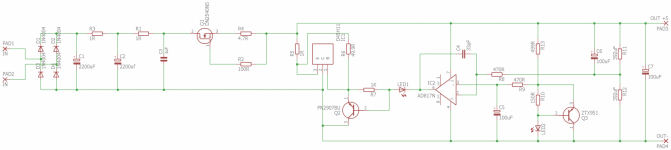
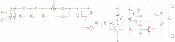
Hi everyone, I intend to design some pcb for Mr. Walt Jung's shunt, I took the original schematic and added the reference GLED431. My idea is to design a pcb schematic and then make it public for those who want to print it themselves or modify it since there are none. I share the schematic I created, I would like to know if there are improvements to be made and if you need to have specific precautions in the design phase of the pcb. The PCBs that will then be created will have the rectifier part on board, and perhaps even a transformer for each branch. But let's go in order before we establish the goodness of the scheme ...
For reference : https://refsnregs.waltjung.org/.
For reference : https://refsnregs.waltjung.org/.
Attachments

È anche un'idea. Ho rispettato i componenti originali scelti da Walt Jung. Lo terrò presente. Ora mi concentro su una prima bozza del PCBSei,
Perché non utilizzare un LM317MDTRKG per sostituire il DN2540 è davvero più economico e richiede solo 1 resistore per limitare la corrente; ed è buono fino a 40 volt in ingresso... il tuo AD817 ha una tensione di alimentazione max. ±18 V
Divertiti!
Ok, I just did a series of shunt reg versions for my UGS preamp (+24V & -24V) ; did you look at these:
https://www.diyaudio.com/community/...-retrofit-upgrade-any-317-based-v-reg.331491/
https://linearaudio.nl/superregs
Take care!
https://www.diyaudio.com/community/...-retrofit-upgrade-any-317-based-v-reg.331491/
https://linearaudio.nl/superregs
Take care!
Attachments
walt jung shunt
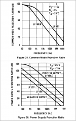
An Improved Reference Filter for Audio Regulators
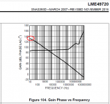
For +/-5V good op amp. is LT6202 , OPA1611 or jfet OPA1641 , low noise jfet op. amp is the best choice.
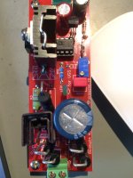
Tix88 ,new improvements from Walt Jung should be out soon, so you should wait a little longer to make a PCB that doesn't look like mine with four extra small PCB (two CCSs and two new version of GLED431)
An Improved Reference Filter for Audio Regulators
For +/-5V good op amp. is LT6202 , OPA1611 or jfet OPA1641 , low noise jfet op. amp is the best choice.
Tix88 ,new improvements from Walt Jung should be out soon, so you should wait a little longer to make a PCB that doesn't look like mine with four extra small PCB (two CCSs and two new version of GLED431)
Attachments
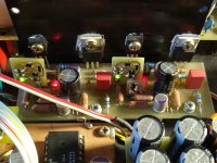
I saw your realization really well done, I will look forward to the new improvements, I could then modify the schemes and make a 2.0 version of the pcb if it will be worth it. Have you noticed any improvements by inserting the css for the Gled cell, instead of the R?walt jung shunt
An Improved Reference Filter for Audio Regulators
For +/-5V good op amp. is LT6202 , OPA1611 or jfet OPA1641 , low noise jfet op. amp is the best choice.
Tix88 ,new improvements from Walt Jung should be out soon, so you should wait a little longer to make a PCB that doesn't look like mine with four extra small PCB (two CCSs and two new version of GLED431)
Hi, thanks for the info. All advice is welcome. What do you think of the scheme? would you make any improvements? I use these power supplies, for the digital and analog part of the Dac chip, and for the digital part of his receiver.I offer the gentle suggestion that you consider using a different opamp, one whose dominant pole rolloff corner is well below (2 x mainsFrequency), i.e., below 100 Hz.
_
I started with the improvements as you did with GLED431, later Walt advised me on new improvements . All the improvements we have made affect the performance of the regulator (shunt or serial) and are heard in the overall sound of the system. I use my regulators in my DAC for six PCM1702 and PMD100.I saw your realization really well done, I will look forward to the new improvements, I could then modify the schemes and make a 2.0 version of the pcb if it will be worth it. Have you noticed any improvements by inserting the css for the Gled cell, instead of the R?
Gled cell work better with CCS and you can always add small pcbs with improvements like me or make new pcb.
I understand your reasoning. I have seen your schematics, they look really good, I might as well take a cue, using non SMD parts, I would only use SMD parts for upgrades like you did. A good non-SMD part for Gled's CSS which one would you recommend?I started with the improvements as you did with GLED431, later Walt advised me on new improvements . All the improvements we have made affect the performance of the regulator (shunt or serial) and are heard in the overall sound of the system. I use my regulators in my DAC for six PCM1702 and PMD100.
Gled cell work better with CCS and you can always add small pcbs with improvements like me or make new pcb.
There are packed JFET CCS in form of, so called, Current Regulator Diode. They are available, cheap and with excellent performance, in no way inferior to discrete JFET CCS. It is possible to get over 160 dB PSRR at voltage reference, before any further filtering.
Improving simple CCS PSRR
Improving simple CCS PSRR
Here's a couple of suggestions if I may, not wishing to overcomplicate things but to gain measurable performance improvement. Not shown on the schematic is the necessary decoupling of the opamp supply pins. A 100nF X7R ceramic at pins 7 and 4 would be good. You might want to consider some RC decoupling of the positive supply pin 7 as well. A 1uF polyester (say Wima MKS series) fed through a 1 to 4.7 ohm resistor would drop only a few mV of supply but give even better decoupling. Replacing R13 with a CCS is a nice idea but with only 2.5 volts available and a 5 mA supply required for the GLed that won't work as you will get a low output voltage. An alternative is a simple single LED and transistor current source that would operate better at that voltage, set for at least 5mA. Suggest a 2N2907, a green LED and a 200 ohm resistor for this. Be careful to not specify low ESR capacitors for C6 and C7 to avoid potential oscillation, perhaps even consider pads for low value resistors in series with each of these to open up the options. Q1 is great and will be less noisy than an LM317 and although that may be insignificant why risk it. Q1 can be cascoded with a second DN2540 for even better performance. Walt Jung detailed this in one of the addendums to his Sources 101 series. Shunt regulators lend themselves quite nicely to upstream choke filtering (CLC). You're probably looking at approx 200mA with R4 at 4.7R so a Hammond 156R would work but you would need 10 more volts on C1 to start with, i.e. a higher voltage transformer. You also need to ensure enough Drain to source voltage across Q1 to ensure it is in the linear constant current region and giving a high output impedance for good line regulation. Looking at the data sheet that will mean at least 10 volts across it. You can get away with less but its performance will suffer. Q1 may be dissipating as much as 2W so will need a small heatsink to avoid getting toasty.
Finally to allow use of a greater range of opamps I would suggest a dual DIP and SOIC layout where the SOIC footprint and pads sit within the DIP one. With source impedances of 470R you will get the lowest noise with bipolar opamps such as my favourite with a 5 volt rail, the OPA1611.
Lots of options. Take your pick.
John
Hello . Thanks for all this good info, change the schematic with these changes and propose it again. What type of capacitor C3 is it advisable to put it?Ecco un paio di suggerimenti se posso, non desiderando complicare eccessivamente le cose ma ottenere un miglioramento misurabile delle prestazioni. Non mostrato nello schema è il necessario disaccoppiamento dei pin di alimentazione dell'opamp. Una ceramica X7R da 100 nF ai pin 7 e 4 sarebbe buona. Potresti prendere in considerazione anche un disaccoppiamento RC del pin di alimentazione positivo 7. Un poliestere da 1uF (diciamo Wima serie MKS) alimentato attraverso un resistore da 1 a 4,7 ohm ridurrebbe solo pochi mV di alimentazione ma darebbe un disaccoppiamento ancora migliore. Sostituire l'R13 con un CCS è una buona idea ma con solo 2,5 volt disponibili e un'alimentazione di 5 mA richiesta per il GLed che non funzionerà poiché otterrai una bassa tensione di uscita. Un'alternativa è un semplice LED singolo e una sorgente di corrente a transistor che funzionerebbe meglio a quella tensione, impostata per almeno 5 mA. Suggerisci un 2N2907, un LED verde e una resistenza da 200 ohm per questo. Fare attenzione a non specificare condensatori ESR bassi per C6 e C7 per evitare potenziali oscillazioni, forse anche considerare pad per resistori di basso valore in serie con ciascuno di questi per aprire le opzioni. Q1 è ottimo e sarà meno rumoroso di un LM317 e anche se potrebbe essere insignificante, perché rischiare. Q1 può essere cascoded con un secondo DN2540 per prestazioni ancora migliori. Walt Jung lo ha dettagliato in uno degli addendum alla sua serie Sources 101. I regolatori shunt si prestano abbastanza bene al filtraggio dell'induttanza a monte (CLC). Probabilmente stai guardando circa 200 mA con R4 a 4,7 R, quindi un Hammond 156R funzionerebbe ma avresti bisogno di 10 volt in più su C1 per cominciare, cioè un trasformatore di tensione più alto. È inoltre necessario garantire una quantità sufficiente di Drain to source su Q1 per garantire che si trovi nella regione di corrente costante lineare e fornisca un'impedenza di uscita elevata per una buona regolazione della linea. Guardando la scheda tecnica, ciò significherà almeno 10 volt su di esso. Puoi farla franca con meno, ma le sue prestazioni ne risentiranno. Q1 potrebbe dissipare fino a 2 W, quindi sarà necessario un piccolo dissipatore di calore per evitare di diventare tostato.
Infine, per consentire l'uso di una gamma più ampia di amplificatori operazionali, suggerirei un layout dual DIP e SOIC in cui l'impronta SOIC e i pad si trovano all'interno di quello DIP. Con un'impedenza della sorgente di 470R otterrai il rumore più basso con amplificatori operazionali bipolari come il mio preferito con un rail da 5 volt, l'OPA1611.
Molte opzioni. Fai la tua scelta.
John
For C3 a low ESR electrolytic would be fine. Boutique plastic caps won't make any noticeable difference here IMHO. What you change/add on the schematic very much depends on where you are pitching this. There is always the option of linking out some of the additions to start with, the CCS for example, and then installing those bits later on, otherwise you may either never get round to trying them or be forced to use added daughter boards (a la Grunf).
John
John
Last edited:
I will use the power supply to power the analog art of the DAC chip, the digital part of the DAC chip, and the power supply of the receiver. In total I need 2 power supplies for the analog part +5/0/-5, and 5 for the digital part +5. I would like to make a modular and at least definitive design, so as not to modify the PCBs much in the future.For C3 a low ESR electrolytic would be fine. Boutique plastic caps won't make any noticeable difference here IMHO. What you change/add on the schematic very much depends on where you are pitching this. There is always the option of linking out some of the additions to start with, the CCS for example, and then installing those bits later on, otherwise you may either never get round to trying them or be forced to use added daughter boards (a la Grunf).
John
Tiziano
Well then it can help you, I need it to power my dac I'm building, with the ad1865 chip.Watching this thread with great interest to use with my AD1862 dac. +/-5v and +/-12v are required for the dac board.
I made the changes you suggested to the scheme, what do you think?Here's a couple of suggestions if I may, not wishing to overcomplicate things but to gain measurable performance improvement. Not shown on the schematic is the necessary decoupling of the opamp supply pins. A 100nF X7R ceramic at pins 7 and 4 would be good. You might want to consider some RC decoupling of the positive supply pin 7 as well. A 1uF polyester (say Wima MKS series) fed through a 1 to 4.7 ohm resistor would drop only a few mV of supply but give even better decoupling. Replacing R13 with a CCS is a nice idea but with only 2.5 volts available and a 5 mA supply required for the GLed that won't work as you will get a low output voltage. An alternative is a simple single LED and transistor current source that would operate better at that voltage, set for at least 5mA. Suggest a 2N2907, a green LED and a 200 ohm resistor for this. Be careful to not specify low ESR capacitors for C6 and C7 to avoid potential oscillation, perhaps even consider pads for low value resistors in series with each of these to open up the options. Q1 is great and will be less noisy than an LM317 and although that may be insignificant why risk it. Q1 can be cascoded with a second DN2540 for even better performance. Walt Jung detailed this in one of the addendums to his Sources 101 series. Shunt regulators lend themselves quite nicely to upstream choke filtering (CLC). You're probably looking at approx 200mA with R4 at 4.7R so a Hammond 156R would work but you would need 10 more volts on C1 to start with, i.e. a higher voltage transformer. You also need to ensure enough Drain to source voltage across Q1 to ensure it is in the linear constant current region and giving a high output impedance for good line regulation. Looking at the data sheet that will mean at least 10 volts across it. You can get away with less but its performance will suffer. Q1 may be dissipating as much as 2W so will need a small heatsink to avoid getting toasty.
Finally to allow use of a greater range of opamps I would suggest a dual DIP and SOIC layout where the SOIC footprint and pads sit within the DIP one. With source impedances of 470R you will get the lowest noise with bipolar opamps such as my favourite with a 5 volt rail, the OPA1611.
Lots of options. Take your pick.
John
Attachments
- Home
- Amplifiers
- Power Supplies
- Walt Jung shunt Design