Hi Andrew
Yes, that pretty well summarises how I think it works.
I don't think the lower diode drop of the hotter diode makes any material difference to the effective turn off of the transistor.
I think it is to address your first concern, that the bias is influenced in two places and potentially they could conflict.
But if all the diodes are thermally matched then at least they should track and minimize the problem.
I share your concern about the principle, "a parameter should be set in exactly one place" is fundamental to database (my profession).
But I believe the circuit should work fine, it looks reasonably tolerant.
However I haven't used it in an amp, my baseline 100 W only uses one pair of Thermal Trak so I don't have any spare diodes.
But I trust Damir if he says it works in his experience.
Best wishes
David
... then when the lower devices start to come ON and the upper devices are still ON...current to be pulled from the upper base terminal.
Yes, that pretty well summarises how I think it works.
...If the driver TT diodes were not thermally coupled, then that fixed diode voltage would not get best performance at sucking charge out of the opposite base. By using a thermally coupled diode the hot device needs a lower diode drop to help suck out that charge and thus switch OFF the opposite device a bit quicker.
Whereas a cold diode would have a higher voltage and thus pull less current out of the fast changing ON to OFF base terminal. Leaving that transistor to run hotter still?
I don't think the lower diode drop of the hotter diode makes any material difference to the effective turn off of the transistor.
I think it is to address your first concern, that the bias is influenced in two places and potentially they could conflict.
But if all the diodes are thermally matched then at least they should track and minimize the problem.
I share your concern about the principle, "a parameter should be set in exactly one place" is fundamental to database (my profession).
But I believe the circuit should work fine, it looks reasonably tolerant.
However I haven't used it in an amp, my baseline 100 W only uses one pair of Thermal Trak so I don't have any spare diodes.
But I trust Damir if he says it works in his experience.
Best wishes
David
Last edited:
Thanks for the three posts with explanation.
I'll summarise as I am understanding what has been posted:
The Vbe Multiplier with the two TT diodes sets the bias voltages for all the output stages.
Since the Driver emitter diodes do not have much "bias voltage" influence, they must be set to a higher bias voltage and so effectively idle along doing almost nothing other than passing the driver bias current.
When the output stage is outputting a little bit, (still in ClassA) the driver diodes don't bring much to the table. They are still idling along and the output base to base bias voltage remains roughly steady.
When the output stage is into ClassB and the output devices take large base currents and charge up the base capacitance, especially at higher frequencies, then when the lower devices start to come ON and the upper devices are still ON, the lower driver goes low in drive voltage and the fixed diode drop + low value emitter resistor allow a large current to be pulled from the upper base terminal.
One bit I will have a quess at:
If the driver TT diodes were not thermally coupled, then that fixed diode voltage would not get best performance at sucking charge out of the opposite base. By using a thermally coupled diode the hot device needs a lower diode drop to help suck out that charge and thus switch OFF the opposite device a bit quicker.
Whereas a cold diode would have a higher voltage and thus pull less current out of the fast changing ON to OFF base terminal. Leaving that transistor to run hotter still?
Andrew, I think that you summarized that quite well, better than I could.
Damir
See, there was no disagreement.
It was a case of "I could not understand what you were showing".
As I have said many times, I am not good at AC design. I suspect I will keep on learning till I can't learn any more.
I wish I could get a proper handle on LTspice. I have a amp on the bench and have now given up trying to find an oscillation on the -ve sinewave peak just a tiny fraction before visible clipping. Once I had found that, I went back to the squarewave to discover it was there on the -ve side as well. But it occurred for a tiny bit of input signal range and I had missed activating the oscillation by my usual methods of testing squarewaves. I don't usually test squarewaves at almost the clipping level of the amplifier !
These PCBs will go on the shelf until I learn more.
See, there was no disagreement.
It was a case of "I could not understand what you were showing".
As I have said many times, I am not good at AC design. I suspect I will keep on learning till I can't learn any more.
I wish I could get a proper handle on LTspice. I have a amp on the bench and have now given up trying to find an oscillation on the -ve sinewave peak just a tiny fraction before visible clipping. Once I had found that, I went back to the squarewave to discover it was there on the -ve side as well. But it occurred for a tiny bit of input signal range and I had missed activating the oscillation by my usual methods of testing squarewaves. I don't usually test squarewaves at almost the clipping level of the amplifier !
These PCBs will go on the shelf until I learn more.
In my opinion you knowledge about electronic is quite high, don't be afraid of a simulations. I start to use LTspice some years ago(I am 70 years old so newer to late) and it is quite user friendly. Just try different combination and use you electronic understanding, haw else we can tray so many different amp, to build it? NO.
AndrewT brought up a good question. The pinout for the JFETs. How can I tell which is the drain and which is the source in your schematic? Also, is it important that the two JFETs be thermally coupled?
I hope you meant the layout as in schematic is standard how to draw nfet. Up - Drain, Erow - Gait, Down - Source.
Look the attached layout, LSK389 has marked pins, S1, D1, G1 - S2, D2, G2.
Problem is with individual LSK170(2SK170) the pinout, S, G, D, you will need some pins bending to accommodate two fets in the position of dual fet. Try to thermally couple them if you can, but more important is to match two fets Idss.
BR Damir
Attachments
Hi, Dado,
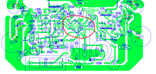
I'm close to finishing populating the boards. I'm having trouble finding a couple resistors on the Schematic. There are two R35. One attached to the vbe and one next to Rx. Neither that R35 nor Rx are on the Schematic. Can you tell me what to use for those?
Thanks, Terry
I'm close to finishing populating the boards. I'm having trouble finding a couple resistors on the Schematic. There are two R35. One attached to the vbe and one next to Rx. Neither that R35 nor Rx are on the Schematic. Can you tell me what to use for those?
Thanks, Terry
Hi, Dado,
I'm close to finishing populating the boards. I'm having trouble finding a couple resistors on the Schematic. There are two R35. One attached to the vbe and one next to Rx. Neither that R35 nor Rx are on the Schematic. Can you tell me what to use for those?
Thanks, Terry
Hi Terry,
R35 attached to Vbe is 6k8, R35 and C22 next to Rx don't populate(they are not on the last schematic), and instead Rx put short connection, jumper. Last schematic is here. http://www.diyaudio.com/forums/solid-state/182554-thermaltrak-tmc-amp-27.html#post4165464
Did you get input fet? If any problem, just ask any time.
BR Damir
Hi Damir,
I saw that they were missing on the Schematic but even the latest layout you posted has those parts. I will do as you say. I was unable to find the dual fet you specified. I plan to use two k170s.
Thanks, Terry
Terry, I have LSK 389 in a SMD, do you want them?
Hi Damir,
I saw that they were missing on the Schematic but even the latest layout you posted has those parts. I will do as you say. I was unable to find the dual fet you specified. I plan to use two k170s.
Thanks, Terry
All those components are there to have possibility to try a bit different compensation. R35 paralleled to C22 are to have some local NFB around VAS(it lowers LG), and I did not get any perceivable sound change, but that's me, maybe you can try that if you like, but everything is working without it.
Try to match the k170 for Idss.
Damir
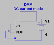
Apply voltage with the gate and source shorted, and measure Id. Use the same Vds that it will have in the intended circuit.
Thanks Kean, I was to slow.
Vds is about 4 V, two green LEDs.
Last edited:
Terry, I have LSK 389 in a SMD, do you want them?
HI Krisfr,
Sorry, I didn't see your post. SMD would be difficult to solder into this board. I had better stick with the K170s.
Thanks kean for the drawing. I understand now I used a similar circuit for matching vgs of some mosfets for some of the amps I've built.
Blessings, Terry
Here.
Sorry if this is a dumb question, but do I need a resistor to limit the current through the two green leds? What voltage do I need to feed the circuit?
Sorry if this is a dumb question, but do I need a resistor to limit the current through the two green leds? What voltage do I need to feed the circuit?
There is a CCS(Constant Current Source) containing M1 depletion mode MOSFET DN2535, R42=470R and R34=100R feeding those green LEDs. I noticed now that wrongly this MOSFET is called J3 on the PCB you are using. This PCB can accept TO92 or SMT mosfet. If you don't have this depletion mode mosfet you can use 12K for R42 and put a jumper between the drain and the source on the PCB instead.
Damir
- Status
- This old topic is closed. If you want to reopen this topic, contact a moderator using the "Report Post" button.
- Home
- Amplifiers
- Solid State
- ThermalTrak+TMC amp