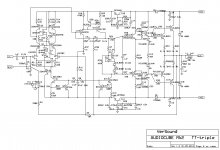
As I have had some request for the PCB and there is an error in the bias setting, here is correct schematic and the PCB layout.
Any question's welcome.
Damir
Any question's welcome.
Damir
Attachments
Nice!What are D7 and D8 for?...
Damir looks to be off-line so if I may answer.
D7 and D8 are to assist turn-off of the outputs.
They make it possible to reduce the value of R13, so the opposite driver can pull current out more effectively.
Best wishes
David
I would not call it linearising.
I see the Vbe multiplier as setting up bias voltages for ALL the following stages.
I also see D7 & 8 + R13 as setting up a bias voltage for the output stage only.
That to me is a conflict.
Both the Vbe multiplier AND D7&8 are trying to set the bias voltage for the output stage.
It could be that one is actually setting up the output stage bias and the other is preventing an overvoltage, i.e. operating as a "set bias" plus protect.
There are various schemes that try to compensate for the non-linear V/I relation in a transistor with a diode.
This isn't one of them, so I wouldn't call it "linearisation".
It just makes use of the temperature co-efficient of the diodes matched (more or less) to the transistor.
But I don't want to pre-empt Damir's answer, just jumped in so you didn't have to wait.
Best wishes
David
This isn't one of them, so I wouldn't call it "linearisation".
It just makes use of the temperature co-efficient of the diodes matched (more or less) to the transistor.
But I don't want to pre-empt Damir's answer, just jumped in so you didn't have to wait.
Best wishes
David
Last edited:
Damir looks to be off-line so if I may answer.
D7 and D8 are to assist turn-off of the outputs.
They make it possible to reduce the value of R13, so the opposite driver can pull current out more effectively.
Best wishes
David
Thank you David, it is exactly like this, Cordell showed it in one of the TT thread. Andrew does not agree as I see. It could be replaced with parallel combination of resistor and capacitor (most common used solution) but here two TT diode are spare and why not use it in the best way.
Best wishes and Happy New Year
Damir
Which is setting the output stage bias voltage?
I have stated two scenarios. I don't know which applies. That is not disagreement !!!!!!
You do not see.Andrew does not agree as I see.
I have stated two scenarios. I don't know which applies. That is not disagreement !!!!!!
Which is setting the output stage bias voltage?You do not see.
I have stated two scenarios. I don't know which applies. That is not disagreement !!!!!!
I'll try to explain it how I understand this.
The bias is set with P1. The diodes in the drivers emitters, of course influence the bias current, but not so much, the TT diode tempco is lower than those of the output transistors, specially at higher current used here, so the main thermal compensation is coming from the TT diodes in the Vbe multiplier. There is question to balance this thermal compensation. My TT amp has quite stable thermal behavior, just a bit overcompensated.
Those diodes does not protect against overvoltage here, just do what David explained, but better then ordinary diodes not thermally connected to the output transistors.
I hope my observation is correct enough, but here are people with much better electronic knowledge and command of English.
As I have had some request for the PCB and there is an error in the bias setting, here is correct schematic and the PCB layout.
Any question's welcome.
Damir
Hi Damir,
Can you please show how to edit/correct the boards from post 166 so i don't have to throw them away and start over? I just finished etching and drilling two new boards when you noted that there were errors. You told me you had a working amp so there must be a way to fix them.
Thanks, Terry
Hi Terry,
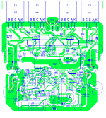
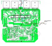
You are so quick that you made the boards before I could give you correct one. Actually I used double side layout(you could find that from the photos) and the PCB correction is very similar to this one. Cut the traces where I marked in red, connect the traces where I connected in blue and remove R44 and connect R35 showed in blue. I hope it's clear, but put it simple P1 and R44(in new sch R35) just interchanged the positions, and that with new values, P1 =2k, R35 =6k8.
Best wishes
Damir
Attachments
Last edited:
Hi Dadod,
What is the amplifier PCB's size?
Thanks
120 x 130 mm.
Hi Damir,
OK I have had time to look it over and it looks like I can just swap the trimmer and R44 and not need to cut any traces. I'll just drill a small hole for the center pin of the trimmer and tie the legs together. Should be simple enough. I'll try to get to it today.
Blessings, Terry
OK I have had time to look it over and it looks like I can just swap the trimmer and R44 and not need to cut any traces. I'll just drill a small hole for the center pin of the trimmer and tie the legs together. Should be simple enough. I'll try to get to it today.
Blessings, Terry
So I'm doing more reading and I see that I need an LSK389. I can't find those. Where can I get a pair and if not, can it be replaced with two jfets?
LSK289 is from Linear Systems || Home and can be replaced with two LSK170B or LSK170C, or Thoshiba's 2SK170BL.
BR Damir
.................
D7 and D8 are to assist turn-off of the outputs.
They make it possible to reduce the value of R13, so the opposite driver can pull current out more effectively..............
There are various schemes that try to compensate for the non-linear V/I relation in a transistor with a diode.
This isn't one of them, so I wouldn't call it "linearisation".
It just makes use of the temperature co-efficient of the diodes matched (more or less) to the transistor......................
Thanks for the three posts with explanation..................................The bias is set with P1. The diodes in the drivers emitters, of course influence the bias current,...............
Those diodes does not protect against overvoltage here, just do what David explained, but better then ordinary diodes not thermally connected to the output transistors......................
I'll summarise as I am understanding what has been posted:
The Vbe Multiplier with the two TT diodes sets the bias voltages for all the output stages.
Since the Driver emitter diodes do not have much "bias voltage" influence, they must be set to a higher bias voltage and so effectively idle along doing almost nothing other than passing the driver bias current.
When the output stage is outputting a little bit, (still in ClassA) the driver diodes don't bring much to the table. They are still idling along and the output base to base bias voltage remains roughly steady.
When the output stage is into ClassB and the output devices take large base currents and charge up the base capacitance, especially at higher frequencies, then when the lower devices start to come ON and the upper devices are still ON, the lower driver goes low in drive voltage and the fixed diode drop + low value emitter resistor allow a large current to be pulled from the upper base terminal.
One bit I will have a quess at:
If the driver TT diodes were not thermally coupled, then that fixed diode voltage would not get best performance at sucking charge out of the opposite base. By using a thermally coupled diode the hot device needs a lower diode drop to help suck out that charge and thus switch OFF the opposite device a bit quicker.
Whereas a cold diode would have a higher voltage and thus pull less current out of the fast changing ON to OFF base terminal. Leaving that transistor to run hotter still?
Last edited:
So I'm doing more reading and I see that I need an LSK389. I can't find those. Where can I get a pair and if not, can it be replaced with two jfets?
Check the datasheets for pin out.LSK289 is from Linear Systems || Home and can be replaced with two LSK170B or LSK170C, or Thoshiba's 2SK170BL.
BR Damir
The k389 pins look like two k170 in a line but with one k170 turned around 180 degrees. This makes it difficult to get thermal coupling.
That's why Euvl made his first dual heatsink for the k170.
I think Euvl still stocks a variety of dual heatsink for the jFETs.
Alternatively, you could glue the flat face of the two k170 (one on each side of the strip a bit like a lover's seat) to a very short strip of copper/aluminium to both cool and couple the two devices.
- Status
- This old topic is closed. If you want to reopen this topic, contact a moderator using the "Report Post" button.
- Home
- Amplifiers
- Solid State
- ThermalTrak+TMC amp