Ok, mas Jofual.
this is the pdf for toner transfer.
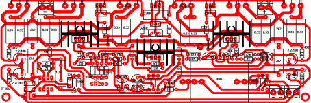
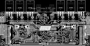
PCB size is 68mm x 200mm (saya kecilkan sedikit)
& you must set "mirror" setting on the printer.
Do have a laser jet printer?
I don't have & tried photocopier but not good, I end up with "spidol" permanent again. I will try another way to make PCB.
No component value!
You must find by your shelf where is component value,
because I usually not make it.
I like PCB without silkscreen
There also .pcb file, but I rename it to .txt
you can try open it with ExpressPCB after rename it again
Enjoy ...
Hi mr John... now I already put all component value.... please you check are all the component value write corectly..?
Attachments
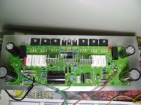
Hi all, thanks to apexaudio for great schematic...
Finally I made SR200 with same value with schematic, here some pictures
(but sorry picture is not good quality)
I use 220nF/63V on VBE & 100pF/100V on colector of the driver transistor
because that what I get here, so what is the maximum voltage that I can use?
Regards
The first design, megusta more.

you could also upload all your data.
thanks.
Attachments
Quick action...Hi mr John... now I already put all component value.... please you check are all the component value write corectly..?
Use 2 x 0.68R/2w not 2 x 0.33R/2w.
I use 1 x 0.33R/5w on my build.
Next I will try 2 x 0.68R/2w & the position is in reverse each other to minimize the inductance, maybe...
thats what I'm thinking.
@SERGIODS,
sorry I don't have with component value...
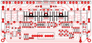
better this new layout
Quick action...
Use 2 x 0.68R/2w not 2 x 0.33R/2w.
I use 1 x 0.33R/5w on my build.
Next I will try 2 x 0.68R/2w & the position is in reverse each other to minimize the inductance, maybe...
thats what I'm thinking.
@SERGIODS,
sorry I don't have with component value...
better this new layout
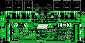
Ok Sir John .. this the new corect one.. and I also corection the resistor 10R from pin 3 IC to ground... thanks for share sir..
Attachments
Thanks for Sharing MR Alex mm.... why the positif and negatif capasitor 470uF not conect to main current sir...?Thanks you Mathez . Files attached .
regards Alex.
Thanks for Sharing MR Alex mm.... why the positif and negatif capasitor 470uF not conect to main current sir...?
I think, they are, connected to main positiv and main negativ rail
whats wrong in your opinion ? 
Alex.
...... sorry , was modified so many times ..... forget to make connection but the silk screen it's the same . In the post#707 it's correct ......
Alex.
but the silk screen it's the same . In the post#707 it's correct ......Alex.
Attachments
Last edited:
...... sorry , was modified so many times ..... forget to make connection
Alex.
Yes Bravo to Mr Alex.... thanks Sir..I like it..very nice pcb layout..
...... sorry , was modified so many times ..... forget to make connection
Alex.
that you are using software to design your "PCBs" ,
Thanks for responding, I will search and download, this program looks very interestingMy software, to design PCB, is Sprint Layout 5.0 with licence, and modified library acording to my necesity
regards Alex.
...... sorry , was modified so many times ..... forget to make connection
Alex.
Hi Alex, I have most of the parts for this amp. Can you please make the pads of Q9, Q7 and Q8 a bit bigger? really appreciated your endless efforts for making a PCB layout which beautifully executed.
BR,
Junie
Last edited:
...... sorry , was modified so many times ..... forget to make connection
Alex.
OT: Alex MM, can you make layout for the super leach here? thanks http://www.diyaudio.com/forums/solid-state/51392-leach-super-amp-pcb-re-design-lsaprd-12.html

- Home
- Amplifiers
- Solid State
- Studio Reference Amplifier