+-24V will probably be enough for my 5W speakers. The room they're in is only what, 8 to 10 feet square? So I don't think I'll need much power for listening.
I see.
But the Allison isn't a switching circuit. The Baker clamp wouldn't help in this situation I think (and I doubt that's what Ken meant).
According to the datsheets, saturation should not be a problem.
http://www.fairchildsemi.com/ds/MM/MMBT2369A.pdf
http://www.datasheetcatalog.org/datasheet/fairchild/PN4258.pdf
These datasheets are what the actually 5771/5769 datsheets said to go to for characteristics.
Is there something I'm missing?
- keantoken
Regarding transistor storage time. It is caused by stored charge in the base emitter junction and in the simulator it is related to Tr. If you look at the base current during the storage time of a transistor you will see a reverse current. The Baker clamp prevents saturation of the CE junction and thus prevents excess charge from accumulating.
I see.
But the Allison isn't a switching circuit. The Baker clamp wouldn't help in this situation I think (and I doubt that's what Ken meant).
According to the datsheets, saturation should not be a problem.
http://www.fairchildsemi.com/ds/MM/MMBT2369A.pdf
http://www.datasheetcatalog.org/datasheet/fairchild/PN4258.pdf
These datasheets are what the actually 5771/5769 datsheets said to go to for characteristics.
Is there something I'm missing?
- keantoken
You're right, storage time should not be an issue in Allison circuits, because Vbc will be greater than zero. I was just responding to this:
"Ken, I assume the storage time has to do with Cob becoming larger as Vce decreases?"
My point is that storage time is caused by base charge, not Cjc.
"Ken, I assume the storage time has to do with Cob becoming larger as Vce decreases?"
My point is that storage time is caused by base charge, not Cjc.
Best start thinking where am I blameless to send this junk?
You got now four 24V 6.5A power supplies, COSEL PBA150F.
But they either need 3 and 5 hump Euro connectors, else or
you gonna have to do some soldering direct to the boards...
Its not got screw terminals like the pic on the spec sheet.
Note there's also an IEC (PC power style) connector brick
with an ON/OFF switch, master fuse, and some line filters.
I'm sending plenty extra pigtail fuses too, use them!!!
Regarding loads: I just melted a set of my alligator clips...
Which reminds me NOT to send 25W load resistors to do a
25W job. May survive, but not the surface its sitting on...
So I'm sending four per channel, you can parallel/series
a quad of them for 100W, but expecting you to cook no
more than 25W though all four. Unless maybe you got a
spare heatsink (from an old PC) you can bolt them to....
Thermal epoxy is good too, if you don't got drills and taps.
JBWeld (steel filled) might do in a pinch...
Last edited:
I am going to go and ask regarding that address sometime around 8:00 I think.
Until then, I hope I've posted something useful in the Software tools forum!!!
http://www.diyaudio.com/forums/showthread.php?p=1910023#post1910023
- keantoken
Until then, I hope I've posted something useful in the Software tools forum!!!
http://www.diyaudio.com/forums/showthread.php?p=1910023#post1910023
- keantoken
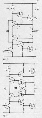
My favorite Allison circuits - part 1
I've been looking at Allison biased circuits for some time (2 years naybe), and while there are numerous ways this bias scheme can be used, I have several personal favorites.
The original article was published by W. Allison in Wireless World of December 1972. The two circuits he presented are attached. The first one (Fig 1) is the normal `Sliding Class A Bias' scheme which works very well. The second (Fig 2) was his attempt to reduce the voltage drop across the output resistors from one Vbe to 1/2 Vbe.
I've had a few attempts at getting the Fig 2 circuit to work, but I think that there is too many devices in the feedback loop and hence too much phase shift at high frequencies. It would be hard to make this circuit stable into typical loudspeaker loads.
My preferred Class A output stage is to incorporate the Bryston Quad-Complementary output transistor arrangement (see the second attachment). Here it is shown as a Class A headphone output stage, but changing the devices and using a suitable Re value would make a small and simple Class A output stage for loudspeakers. This circuit can be voltage driven as shown, or current driven by varying I1 and I2 (ie a typical VAS stage). Note - don't allow this circuit to go into Class B mode, as the Mosfet drivers turn off and inject horrible transients into the signal.
That's enough for these circuits, continued in part 2.
Paul Bysouth, September 2009.
Attachments
My favorite Allison circuits - part 2
My next favorite is a buffered input version that provides very high imput impedance.
In the attached circuit I've shown, as well as the Allison bias scheme, a means of implementing an offset correction scheme (V4 would typically be an Opamp integrator).
Note that this circuit has two Vbe drops across each Re resistor, and hence would not be suitable for driving loudspeakers. This circuit would however, be ideal as a preamplifier output or headphone amplifier.
Also do not let this circuit go into Class B mode, as one of the two input transistors (Q2, Q4) will turn off, and probably go unstable (highly distorted at least).
Continued in part 3 ...
Paul Bysouth, September 2009
Attachments
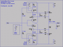
My favorite Allison circuits - part 3
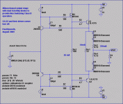
The normal Allison `Sliding Class A Bias' scheme really only works for Class A (ie neither output transistor ever turns off), and if a transient pushes it into Class B operation, the distortion increases dramatically.
I've been looking for a suitable modification to allow Class A/B operation, and after many false starts arrived at the circuit show in the attachment.
The addition of two Schottky diodes (thanks to Kenpeter for prompting me to relook at this arrangement, but this time with Schottky diodes rather than Silicon diodes) provide a smooth transition into Class B operation. The addition of the resistor R1 ensures that the Allison bias `stays alive', and that Q3,Q4 nerver turn off. Similarly R2 ensures that M1,M2 nerver turn off. This circuit becomes a form of `Non Switching Class B' output stage.
I've also shown bootstrapped current sources to drive the Allison bias transistors (ie Q1,Q2), and note the inclusion of a diode and a Jfet to set the bias current. I've show C1 being connected to Q3 (and C2 to D4), but it may be preferrable to cross connect C1 to Q4 (and C2 to Q3).
I've spend some time downloading and checking many Schottky diode Spice models. Most bear little resemblance to their datasheets! The Onsemi MBR1045 model comes reasonable close, so that The model I've used. I don't expect that the real circuit will match the Spice model, but shouldn't be too far off.
Initially when I thought of using the Schottky diodes and the `keep alive' resistor (ie R1), I was quite pleased, then I reread Nelson Pass' patent 3,995,228 only to discover that he had had a similar idea 30 years before me.
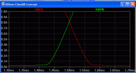
Also attached is a simulation of the currents in the two output transistors during crossover. Note that they don't turn off (though the Schottky diodes will).
After experimenting with this idea for a while, I had a better idea! Continued in Part 4.
Paul Bysouth, September 2009.
The normal Allison `Sliding Class A Bias' scheme really only works for Class A (ie neither output transistor ever turns off), and if a transient pushes it into Class B operation, the distortion increases dramatically.
I've been looking for a suitable modification to allow Class A/B operation, and after many false starts arrived at the circuit show in the attachment.
The addition of two Schottky diodes (thanks to Kenpeter for prompting me to relook at this arrangement, but this time with Schottky diodes rather than Silicon diodes) provide a smooth transition into Class B operation. The addition of the resistor R1 ensures that the Allison bias `stays alive', and that Q3,Q4 nerver turn off. Similarly R2 ensures that M1,M2 nerver turn off. This circuit becomes a form of `Non Switching Class B' output stage.
I've also shown bootstrapped current sources to drive the Allison bias transistors (ie Q1,Q2), and note the inclusion of a diode and a Jfet to set the bias current. I've show C1 being connected to Q3 (and C2 to D4), but it may be preferrable to cross connect C1 to Q4 (and C2 to Q3).
I've spend some time downloading and checking many Schottky diode Spice models. Most bear little resemblance to their datasheets! The Onsemi MBR1045 model comes reasonable close, so that The model I've used. I don't expect that the real circuit will match the Spice model, but shouldn't be too far off.
Initially when I thought of using the Schottky diodes and the `keep alive' resistor (ie R1), I was quite pleased, then I reread Nelson Pass' patent 3,995,228 only to discover that he had had a similar idea 30 years before me.
Also attached is a simulation of the currents in the two output transistors during crossover. Note that they don't turn off (though the Schottky diodes will).
After experimenting with this idea for a while, I had a better idea! Continued in Part 4.
Paul Bysouth, September 2009.
Attachments
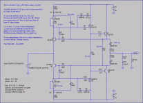
My favorite Allison circuits - part 4
When I was experimenting with the circuit in Part 3, I decided that if a pair of Schottky diodes was a good thing, then two pairs should be even better!
See the attachment for the concept.
Note that the output transistors never turn off, but the Schottky diodes will. Adjust Re to set a suitable bias current. As the Schottky diodes heat up, the bias current will increase (but not run away). Thermally bonding the diodes to Q3,Q4 will produce a stable bias current. To126 transistors for Q3,Q4 would probably be easier (I'm planning to use ksc3503 and ksa1381). The temperatures of Q1, Q2, M1 and M2 have no effect on the bias current.
I'm currently working on a variation of this with a Bryston output stage, and its looking very promising. I've been able to include a current limiter to protect the transistors and diodes, and I've been able to tame the turn on transients. I'll publish the design once its built and tested.
Paul Bysouth, September 2009.
Attachments
Hey Paul,
Regarding zvn3306: For DC curve, zvp2106 is maybe closer compliment.
Close at AC too, if you sandbag n3306 with an equivalent capacitance.
And we aren't talking a whole lot extra... In this app, such sandbagging
probably isn't even needed.
The worst mismatching figure for vp3306 is that it has only 60mS gain.
Compare to 150mS for the vn3306 part, I just can't see using these two
together as compliments... Not when better compliment, vp2106 exists.
I agree the mosfet/bjt Darlington arrangement. Superior to driving big
gated MOSFETs. Especially with unbuffered single emitter comparators.
Straight cascode action from input to gate gives no drive current assist.
So we want that gate cap small as practical.
Buffering helps with both the drive current swing, and input impedance.
And the complimentary series pairing makes vbeebv identical for both.
But such buffering usually widens the diamond, and makes challenges
how best to close the additional voltage gap. I've looked into vdssdv
with JFETs which can have a zero or even negative drop.... Also have
an interest in Germanium BJTs, as vbe is typically only 0.23V.
Hey Paul,
Regarding zvn3306: For DC curve, zvp2106 is maybe closer compliment.
Close at AC too, if you sandbag n3306 with an equivalent capacitance.
And we aren't talking a whole lot extra... In this app, such sandbagging
probably isn't even needed.
The worst mismatching figure for vp3306 is that it has only 60mS gain.
Compare to 150mS for the vn3306 part, I just can't see using these two
together as compliments... Not when better compliment, vp2106 exists.
I agree the mosfet/bjt Darlington arrangement. Superior to driving big
gated MOSFETs. Especially with unbuffered single emitter comparators.
Straight cascode action from input to gate gives no drive current assist.
So we want that gate cap small as practical.
Buffering helps with both the drive current swing, and input impedance.
And the complimentary series pairing makes vbeebv identical for both.
Especially if constructed using one end of each from "matched pairs".
But such buffering usually widens the diamond, and makes challenges
how best to close the additional voltage gap. I've looked into vdssdv
with JFETs which can have a zero or even negative drop.... Also have
an interest in Germanium BJTs, as vbe is typically only 0.23V.
Ohyeah, and I've also fooled with quasicomplimentary vdssdv MOSFETs in the output too.
Was thinking two gate caps in series is only half the capacitance of one, and doesn't add
another "pole" of phase shift. But in reality, Qg seems to be dominant. And even in series,
that figure doubles... So that brilliant idea went nowhere...
Was thinking two gate caps in series is only half the capacitance of one, and doesn't add
another "pole" of phase shift. But in reality, Qg seems to be dominant. And even in series,
that figure doubles... So that brilliant idea went nowhere...
Thanks for your input Paul, I was wondering if you had dropped off the planet. ")
In Part 2, the collector of Q3 can be connected to the source of M2 for a cascoding affect (and the same for Q4). This also allows you to use lower voltage, higher quality parts for this position. IIRC, it also reduces distortion by an insignificant amount (though maybe it won't matter since you're driving MOSFETs).
Well, I went to a pawn shop and got a really heavy dead Onkyo amp for $10. I now am sure I have a adequate heatsink, but I think the HUGE transformer might have too high voltage for the amps. I will have to check. The 12000uF filter caps are rated for 71WV. Output devices were 2SA1493/C3857.
Too bad about picture quality, I took this with a webcam and I can't turn compression off.
- keantoken
Attachments
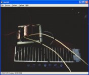
Okay, here are the parts from that find:
HEAVY trafo,
HUGE heatsink,
2x 71WV 12000uF caps
2x 2SA1493 (These look like possible substitutes for the 2SA1943/C5200, but I haven't tested to see if they're good. If even one is dead, I don't want to use them for the boards Hugh sent.)
2x 2SC3857
2SA1695 (I would not substitute these for the 2SA4793/C1837, since they're much slower).
2SC4468
Mica pads for all above transistors.
2x 2SA1725 (6A, 30W, 20MHz. I'll bet these would work great in a linear supply)
2x 2SC4511
All transistors are Sankens.
2x 6.3A Fuses
Power rectifier with associated heatsink
Tone control board with some 2SK246... (use or part out?)
I heard someone around here say that the rectifier should be soldered as close to the trafo as possible, rather than being right on the PCB next to the caps and sensitive circuitry. I'd hate to clip those long leads, so I think I'll wrap them around a core and have a small choke right before the rectifier. Is there anything wrong with these plans?
My biggest trouble with Hugh's boards for now is the capacitors... Some of those are expensive. He sent me some of the more expensive ones, but since then he has chosen better values, which are in his post.
- keantoken
Well, the power BJTs I'm sending ( MJ2955, 2N3055 ) are electrically similar
enough (at DC) that nothing would likely blow up... Not saying would sound
as good with real music, but you never know...
I'll have to review that cap list... I'm sending some, but its even worse of a
random grab than the transistors. There is a Velleman 680 resistor assortment
in the kit, you can probably look up what all values that includes. And a 200
resistor surface mount assortment. I didn't look the values, I'm assuming they
are "typical"...
There are at least four really good polypropylene coupling caps... 6.8uF 100V
If you are doing any surface mount, you are gonna quick find out you need
two irons: One for either end of a part you want to reposition or replace.
Bottle of liquid flux, and maybe a heat gun... I'm not offering or sending any
such tools at this time, just saying you might want to ask around.
Last edited:
Sorry: Velleman 610 resistors e12 series K/RES-E12
And a pair of Stromberg Carlson coupling transformers.
Rated 600ohm:600ohm 2H:2H, for telephones I think...
These are potted in small metal cans.
But I use these full range to isolate line signals from
ground loop hum (and prevent blowing up things).
Very flat, much better than spec. I can provide the
measurements to prove...
You might also want to gut some PC power supplies?
Especially if you want some inductors and rectifiers,
heatsinks and micas. And there's usually at least one
really big 450V cap. Usually the main MOSFET is toast.
Just hit the backside with a propane torch, and let
whatever wants to fall free... Cut the rest out later.
Last edited:
Sorry: Velleman 610 resistors e12 series K/RES-E12
And a pair of Stromberg Carlson coupling transformers.
Rated 600ohm:600ohm 2H:2H, for telephones I think...
These are potted in small metal cans.
But I use these full range to isolate line signals from
ground loop hum (and prevent blowing up things).
Very flat, much better than spec. I can provide the
measurements to prove...
You might also want to gut some PC power supplies?
Especially if you want some inductors and rectifiers,
heatsinks and micas. And there's usually at least one
really big 450V cap. Usually the main MOSFET is toast.
Just hit the backside with a propane torch, and let
whatever wants to fall free... Cut the rest out later.
I have some PC supplies lying around, but those 450V caps are usually small values (size-rating ratio is not economical for me). The biggest problem I have with mining components is that the leads are usually cut too small for my breadboard. So apart from the nice toroid(s) and inductors I haven't been enthusiastic about ripping them apart. I haven't tried winding my own mains transformers... Maybe I should.
I'm planning on getting a nice Weller WES51 iron (but if anyone has any offers, I'm all ears). Beyond that I want to construct my own hot air iron... Which should work very well for desoldering components with many leads.
- keantoken
Last edited:
Okay... Allison update!
I just found an awesome variation that sims spectacularly, of course.
I tried this on a whim, and discovered that the Jfets increase transconductance by a huge amount, apparently.
I added the Diamond input buffer just for kicks, and according to the simulator I get about 50Gohms input impedance... Better than my Fluke 8800A. This, with virtually no distortion at 100KHz. Bandwidth is 10MHz! It gets slowly less believable (but then how do the DMM manufacturers do it?). As Kenpeter said, the models probably don't take into account Jfet capacitance distortion though.
The second circuit is an adaptation to use only 2 CCSs, though it's not quite as good.
- keantoken
Attachments
- Status
- This old topic is closed. If you want to reopen this topic, contact a moderator using the "Report Post" button.
- Home
- Amplifiers
- Solid State
- Simulation Analysis of several unique Allison-based output stages.