Tweaking symmetry in the superfast... No special reason why.
It was working fine, no point screwing with it, so I did...
You had one CCS at 5.3mA the other at 6.3mA, balanced that.
Also you had dissimilar transistor pairs up front. I made both
series emitter pairs quasi-complimentary BC557+BC547...
It didn't help or hurt. Like I said, just pointless nittweakage...
Attachments
kenpeter said:Whist lookin for 2N5564 .model, I find post by AuroraB suggesting
that Erno Borberly liked to abuse National Semiconductor AH5020
as the complimentary matched pair... I don't know truth or fiction,
I'm just repeating a rumor, and poorly...
Since its an older chip, might be worth another trip to Tanner to
see if that one was also on the shelf and I just overlooked it?
Didn't see matched pairs of P-JFETs, easily recognized as such.
Doesn't mean they weren't there, staring me square in the face...
True. But they are not complimentary in the package, just one flavor
The compliments start with "NPDxxxx" iirc...

_-_-bear
kenpeter said:I've just read that reverse biasing VBE into reverse breakdown
(like a
I also wonder if this abuse can be deliberately applied to a single
emitter junction transistor to tweak a match? I've never heard of
anyone doing it on purpose, other than as an el-cheapo Zenier
substitute that will never again see service as amplifying device...
The abuse generates hot carriers and the effect is of doubtful stability.
kenpeter said:Tweaking symmetry in the superfast... No special reason why.
It was working fine, no point screwing with it, so I did...
You had one CCS at 5.3mA the other at 6.3mA, balanced that.
Also you had dissimilar transistor pairs up front. I made both
series emitter pairs quasi-complimentary BC557+BC547...
It didn't help or hurt. Like I said, just pointless nittweakage...
Exploration is great catalyst for new developments.
My thoughts:
1: I used the BCxxx pairs for the input so as to have greater input impedance. This appeared to have very good results at first but decreased stability and the required compensation.
2: The CCSs were unequal so as to reduce input offset current. With high-impedance sources, 1uA of offset current can do bad things with DC readings.
1: This circuit doesn't seem to care about Hfe except in the output transistors. It is actually better to select transistors for voltage gain. This is why I still use the 5769/5771. However, I haven't tested this specifically in terms of distortion and bandwidth.
3: I might soon be able to go to radioshack, at which point I will (if something neat doesn't catch my eye) buy some veroboard I spotted that is perfect for prototyping exactly this. So I might be able to test it out. However, my scope only goes up to 1MHz (with 10uV precision!
) so I won't be able to do extensive tests on bandwidth.6: I think I have found the perfect output pair candidates:
http://www.datasheetcatalog.org/datasheet/sanyo/ds_pdf_e/2SC3951.pdf
Too bad no spice models.
Can't find anyone who sells them either.

7: I experimented again with changing the input transistors back to the good ol' 5769/5771. The results were better than I expected. Input impedance is tolerable, still much better than my scope. It was also much easier and simpler to get stable. I might have been shooting myself in the foot by putting those BCxxx in. Schematic:
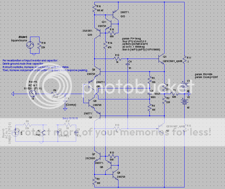
I documented my methods for compensation, as you can see. The blue text refers to the input resistor and C1.
I have attached the .asc file (in txt format). Kenpeter, I see you've caught on to my naming conventions.
- keantoken
Attachments
Look again at again-again: The quasicomp pairs made not only zero
voltage offset in the output, but also zero current offset for the inp.
And that was with current sources manually trimmed to hold the
same quiescent current to either rail...
I was only looking at the output behavior when I first posted...
I'm surprised to find that the input current has no offset also???
Hadn't actually checked that before. I guess the N and P betas
had been chosen fairly close in the models... May not be that
way in real life.
kenpeter said:Look again at again-again: The quasicomp pairs made not only zero
voltage offset in the output, but also zero current offset for the inp.
And that was with current sources manually trimmed to hold the
same quiescent current to either rail...
I was only looking at the output behavior when I first posted...
I'm surprised to find that the input current has no offset also???
Hadn't actually checked that before. I guess the N and P betas
had been chosen fairly close in the models... May not be that
way in real life.
I see.
The BCxxx models I use do have fairly close Hfe between PNP and NPN devices. This said, it is not surprising that they have little offset current. In real life, I would match the gain of the input pair so that little adjustment of the CCS is needed. Since the current gain of the non-input Allison transistors is not important, I would chose these with Vbe values to minimize Vout offset.
It seems that with this circuit, voltage gain of the transistors is far more important than current gain.
This is my next thought. The diodes protect against overinput, keeping the Vbe junction from reverse-biasing. The input transistors shouldn't be affected unless you go over the rails (for use as a scope input I would use much higher rails for the CCS than necessary, just to help ensure no overvoltage problems). I wouldn't prefer to add diodes to the input to protect against over-rail voltage but it couldn't hurt...
- keantoken
Attachments
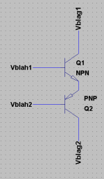
How about AC gain?
As in Vrms(out)/Vrms(in)?
The Allison used with CCSs has lots of voltage gain. Since changing between BCxxx and 5769/5771 transistors has very little effect on distortion performance, I concluded that current gain had very little to do with the performance of this circuit and that a more useful parameter was Ic vs. Vbe (effectively voltage gain, no?).
Of course this will be dependent on the load, but it has proved useful to me when simulating using the Rush Cascode.
For example, using this equation in reference to the attached schematic with an AC analysis, I get what is similar enough to an OLG plot and has worked well enough for me for getting the Allison stable.
V(Vblag1,Vblag2)/V(Vblah1,Vblah2)
(this will not make sense if you use it in a transient analysis - you must run an AC analysis to make use of this equation).
- keantoken
Attachments
keantoken,
The expression I gave is AC gain (volts per volt) at lower frequencies. Note that Ic is the DC operating point. (Yes, gm changes with the DC or instantaneous operating point.) With a CCS load the gain becomes very large (Recall that some time ago I mentioned the very large OLG of your circuits.) So the Rload is the parallel combination of the input impedance of the emitter followers, the output impedance of the CCS and the output resistance of the Allison transistors.
Ic vs. Vbe is called transconductance (gm). Somewhat surprisingly, as a reasonable first order approximation, gm is independent of the specific type of transistor. And Vbe goes up by 60 mV per decade of collector current, and the voltage gain from the base of a CE stage is independent of Hfe. If there is a resistor in series with the base, it's a different story, because the base to emitter resistance (Rb'e) is a function of Hfe.
Rick
sawreyrw said:keantoken,
The expression I gave is AC gain (volts per volt) at lower frequencies. Note that Ic is the DC operating point. (Yes, gm changes with the DC or instantaneous operating point.) With a CCS load the gain becomes very large (Recall that some time ago I mentioned the very large OLG of your circuits.) So the Rload is the parallel combination of the input impedance of the emitter followers, the output impedance of the CCS and the output resistance of the Allison transistors.
Ic vs. Vbe is called transconductance (gm). Somewhat surprisingly, as a reasonable first order approximation, gm is independent of the specific type of transistor. And Vbe goes up by 60 mV per decade of collector current, and the voltage gain from the base of a CE stage is independent of Hfe. If there is a resistor in series with the base, it's a different story, because the base to emitter resistance (Rb'e) is a function of Hfe.
Rick
The THD of the Allison circuit is then a function of the voltage error across the bias resistors, which will depend heavily on the transconductance of the Allison transistors. Unless the load on the Allison transistors becomes large, then output voltage error should be well independent of Hfe. This gives us room to experiment with different transistors regardless of Hfe. Is it possible to find transistors with higher transconductance? These would give the greatest benefit in terms of distortion.
Thanks for clarifying, now I know what transconductance is (it seems you are agreeing with me?).
- keantoken
keantoken,
I don't think I understood the first part of your last post.
Using CCS loads (on the Allisons) with currents well above the current swing in the Allisons will help limit distortion, because the relative change in gm (Ic) will be small. In addition, fT goes up with Ic, to a certain point. So relatively high bias current is good.
gm is a fundamental property of BJTs and it is given by 40*Ic at room temperature. The only way to increase gm is to increase Ic (or temperature).
You might want to spend a little time looking into the hybrid pi model of a BJT. It will give you more insight into all of this. SPICE uses a form of the hybrid pi model.
Rick
Current gain (linear or not) (even if less than unity), is the basis
of all amplifying devices. That is not to say that amplification of
voltage does not occour, only that voltage gained is externally
defined by load and feedback...
Those that are characterised for Voltage Gain (Mu) are linearized
into that domain internally by voltage fed back from the output.
In the case of Triodes, and ceratin Static Induction Transistors
with deep buried gridlike gates: Feedback from the distributed
gradient of carriers in the channel itself, or the space charge of
electrons distributed in a vacuum. External resistors forming a
feedback network are generally not needed. And such intrinsic
feedback is exceptionally fast and "local" in regard to phase.
You hold current steady, and Mu voltage gain is nearly linear.
Thats the normal rule for Vacuum Triodes anyways...
Kinda the opposite of beta, where you hold voltage a steady,
and the current gained is linear... I'm not sure what form of
intrisic feedback a bipolar emitter might make, that it forces
current gained to be as linear as it often is???
I would have expected bipolar devices to act more like FETs,
and have current gain, but no special linearity in either domain.
How exactly they come to have linear beta is a mystery to me.
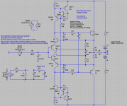
While I think about that, here is a less ambitious application of the Allison as a HF buffer. Simpler is almost always better as far as superfast buffers go.
According to sims, this does -6db at 100MHz. The 1k input resistor causes the circuit to self-limit because of internal capacitance; the value was chosen to be the minimum value where there was no visible distortion at 100MHz.
Input impedance is max, 3.27Mohms (still not bad). 544Kohms at 100KHz. 1Kohms at 100MHz.
The response characteristics of this circuit are much better than the one I have been working on.
Schematic attached.
- keantoken
Attachments
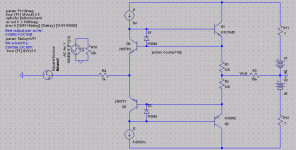
Here's one for Kenpeter.
Maybe you got your inspiration for the diodes from this post? Paul hasn't commented and doesn't seem to do so very often. I was just reviewing the thread and found it.
http://www.diyaudio.com/forums/showpost.php?p=1765270&postcount=22
- keantoken
Maybe you got your inspiration for the diodes from this post? Paul hasn't commented and doesn't seem to do so very often. I was just reviewing the thread and found it.
http://www.diyaudio.com/forums/showpost.php?p=1765270&postcount=22
- keantoken
It predates my first mention of them by several days.
http://www.diyaudio.com/forums/showpost.php?p=1782428&postcount=30
On the other hand, I hadn't heard of Allison at that time.
Didn't yet know that thread might be relevant to me. So
wasn't aware of, nor following any ideas Paul had written.
I found diode AB smoothing independently and by accident.
Did not know for quite a long while exactly why it worked?
If I had read that post of Paul's , would have saved me a
whole lot of head scratching.
And to answers Paul's question regarding his chosen diode
MUR820? I been favoring AB curves of MBR745. Tried several
others, but none ever seemed to cross quite as smooth.
Don't remember anymore if MUR820 was one I tried or not???
Of course, I'm still talking sim preference here, The only real
power Shottkys I have on hand are something else completely...
What I want vs. what I can get locally for cheap.
Last edited:
More junk added to bucket today. Clip on Heatsinks for TO92 and TO220.
Some 3x4 perforated boards with little round solder pad one side each hole.
Supertex small signal mosfets VPsomething-or-other. Compliments I hope.
I had time to cherry pick 2 NPN and 2 PNP Germaniums for matching HFE
NPN 73,73 and PNP 76,77. Possibly this close matching relevant only at
whatever unknown room temperature and current of the HFE meter.
FYI: Random grab, those bins measured like anywhere from 30 to 170.
Some binding posts, RCA jacks, other misc crud I forget...
Ohyeah Qty12 Dale .12ohm 1% wirewounds 2W, and Qty2 7.5ohm 25W...
Enough to drop up to .36ohms per emitter, Stereo... And dummy loads.
They might be a little inductive due to wind, possibly a useful "feature".
Last edited:
Thanks for the parts...
If I pay for shipping, will you send it that way? I imagine the bucket is getting heavy by now...
I am ready now to build up a very nice amplifier (I didn't design it, man am I lucky, got it as a freebie) on some boards... So if you could contact me privately Kenpeter (if you click on my username a menu will open up with that option), I would be willing to pay for what I can.
Now regarding the Germanium transistors for the Allison... The most important factor for choosing these transistors is Gm. So do germaniums have more or less gm than silicon? Google is not my friend in trying to figure this out.
- keantoken
Folks,
Along with many others, I am deeply impressed by Keantoken's contributions here, and I would like him to get something back in return. He's not exactly wealthy, and would greatly benefit from some real components to work with.
I designed a power amp recently using the Rush cascode idea Keantoken came up with. He can take quite a bit of the kudos for this design, which sounds very, very good. I spent some weeks laying out a pcb for the amp (100W into 8R, 190W into 4R) and recently sent a couple of boards to him in Denison TX so he might get to build the results of some of his ideas.
If anyone here, particularly Stateside where postage is cheap, could send a few parts to Keantoken, I'm very sure he would appreciate it. It would also encourage him to continue his worthy contributions, and who knows, come up with another amp or preamp!
Here's a few parts that KT needs:
4 x 0R33 3W 4507 Vishay-Dale smd resistors
4 x 2SC5200 (two matched pairs if possible)
4 x 2SA1943 (ditto)
2 x 2SC4793
2 x 2SA1837
2 x 2SC3423
Four each of the following half watt, MF resistors: 33K, 1K5, 2R2, 12K, 330R, 100R, 2K2, 3K3 (1W), 100K, 10R, 150R, 33R, 22R, 6K8, 10R (1W).
Four each of the following caps: 100uF 63VW, 47uF 50VW, 820p silver mica, 22pF sm, 15pF sm, 100nF 160V MKP, 100nF 100V ps, 2K 3296 bourns trimpot, 200R 3296 bourns trimpot.
I have designed the amp, tested it, laid out a pcb, sent two to him in a simple envelope. He still needs the above parts, which would cost a heap for me to send to the US. If you would like to help, please PM Keantoken (Anthony) to get his mailing address. Be assured that this is a very good cause, KT is just 16 years old, and shows more potential than I've ever seen in a young man of his age. Us wrinklies need to help the fresh-faced designers of tomorrow!
Please give this some thought - generosity would be much appreciated.
Hugh
Along with many others, I am deeply impressed by Keantoken's contributions here, and I would like him to get something back in return.
He's not exactly wealthy, and would greatly benefit from some real components to work with.I designed a power amp recently using the Rush cascode idea Keantoken came up with. He can take quite a bit of the kudos for this design, which sounds very, very good. I spent some weeks laying out a pcb for the amp (100W into 8R, 190W into 4R) and recently sent a couple of boards to him in Denison TX so he might get to build the results of some of his ideas.
If anyone here, particularly Stateside where postage is cheap, could send a few parts to Keantoken, I'm very sure he would appreciate it. It would also encourage him to continue his worthy contributions, and who knows, come up with another amp or preamp!
Here's a few parts that KT needs:
4 x 0R33 3W 4507 Vishay-Dale smd resistors
4 x 2SC5200 (two matched pairs if possible)
4 x 2SA1943 (ditto)
2 x 2SC4793
2 x 2SA1837
2 x 2SC3423
Four each of the following half watt, MF resistors: 33K, 1K5, 2R2, 12K, 330R, 100R, 2K2, 3K3 (1W), 100K, 10R, 150R, 33R, 22R, 6K8, 10R (1W).
Four each of the following caps: 100uF 63VW, 47uF 50VW, 820p silver mica, 22pF sm, 15pF sm, 100nF 160V MKP, 100nF 100V ps, 2K 3296 bourns trimpot, 200R 3296 bourns trimpot.
I have designed the amp, tested it, laid out a pcb, sent two to him in a simple envelope. He still needs the above parts, which would cost a heap for me to send to the US. If you would like to help, please PM Keantoken (Anthony) to get his mailing address. Be assured that this is a very good cause, KT is just 16 years old, and shows more potential than I've ever seen in a young man of his age. Us wrinklies need to help the fresh-faced designers of tomorrow!
Please give this some thought - generosity would be much appreciated.
Hugh
Last edited:
- Status
- This old topic is closed. If you want to reopen this topic, contact a moderator using the "Report Post" button.
- Home
- Amplifiers
- Solid State
- Simulation Analysis of several unique Allison-based output stages.